Effective PCB Design and Fabrication for Precision Electronics

Key Takeaways
In the rapidly evolving field of electronics, effective PCB design and fabrication are foundational for achieving high-quality pcb assembly or PCBA processes. To ensure precision in electronic devices, it is crucial to focus on the pivotal elements that contribute to effective PCB design. This includes understanding the core principles of circuit layout, component placement, and routing techniques that optimize signal integrity and minimize interference. Additionally, leveraging advanced tools and technologies can significantly enhance the efficiency of both the design and fabrication phases. For example, using sophisticated simulation software helps in identifying potential issues early in the development process, thus preventing costly redesigns later. Innovations such as automated assembly techniques are transforming traditional pcb manufacturing, offering enhancements in speed and accuracy that are imperative for modern electronic devices. Overall, adhering to established best practices while remaining open to new ideas will play a crucial role in producing reliable electronics and advancing technological capabilities.

Introduction to PCB Design and Fabrication
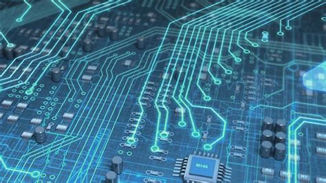
In the modern era of electronics, PCB design and fabrication play a critical role in ensuring the functionality and reliability of devices. A printed circuit board (PCB) serves as the backbone of electronic systems, providing the pathways through which signals and power flow. The process begins with intricate PCB design, where engineers utilize specialized software to map out the components and their interconnections. This design phase is essential for achieving optimal performance in electronic devices, laying the groundwork for subsequent processes.
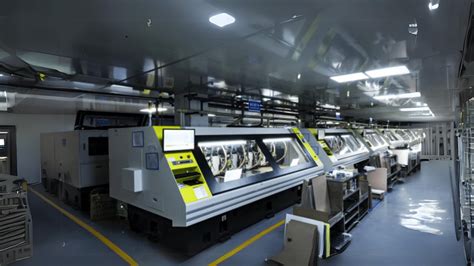
Once the design is validated, fabrication commences. This involves a series of meticulously controlled steps that transform raw materials into a fully functional PCB. Among these steps are etching, layering, and soldering, each crucial for maintaining precision in the final product. One significant aspect of this process is pcb assembly or PCBA, where components are mounted on the board. Utilizing automated techniques such as surface mount technology (SMT) can enhance both efficiency and precision.
To illustrate the importance of these processes, consider a simple table outlining key factors in effective PCB production:
| Factor | Importance |
|---|---|
| Design Accuracy | Ensures all components fit correctly |
| Material Quality | Impacts durability and reliability |
| Assembly Techniques | Affects overall efficiency of production |
| Testing Protocols | Identifies defects before products reach market |
In conclusion, understanding both PCB design and fabrication is imperative for electronics professionals aiming to deliver high-quality devices that meet consumer expectations. Embracing advanced tools and techniques will further enhance these foundational processes while fostering innovation in electronics manufacturing.
Key Elements of Effective PCB Design
Effective PCB design is crucial for ensuring that electronic devices operate reliably and efficiently. At the heart of successful pcb assembly lies a deep understanding of several key elements. First and foremost is the layout, which must optimally position components to minimize signal interference and maximize performance. Designers must pay particular attention to trace width and spacing, as these factors significantly impact the circuit’s electrical characteristics. The use of appropriate materials also plays a vital role; selecting materials with the right dielectric properties can enhance signal integrity.
Moreover, understanding thermal management is essential in pcb design. Effective heat dissipation techniques need to be incorporated into the design to prevent overheating, which could lead to device failure. Employing thermal vias and strategically placed copper planes can help achieve this balance. Additionally, simulation tools have become invaluable in modern pcba processes, allowing designers to predict how their designs will perform under various conditions before fabrication begins.
Another critical aspect involves the selection of components that meet performance specifications while adhering to budget constraints. This involves not only choosing reliable suppliers but also considering lead times and compatibility with existing systems during the initial stages of design development. By integrating these components with precision, engineers can enhance both functionality and durability in their final products.
Ultimately, a comprehensive approach that encompasses layout consideration, thermal management, material selection, and component optimization determines the success of a PCB design initiative. As technology advances, remaining adaptable and integrated within these pcba principles assures continuous improvement in electronic devices across various applications.
Techniques for Precision in PCB Fabrication
Achieving precision in PCB fabrication is crucial for the reliability and performance of electronic devices. The first step is ensuring the design is meticulously executed, utilizing advanced software tools that facilitate simulation and verification of circuit layouts. Techniques such as multi-layer stacking and optimized routing can greatly enhance both space efficiency and signal integrity. Furthermore, employing techniques like controlled impedance routing helps maintain consistency in the electrical performance of the PCB assembly or PCBA.
A key consideration during fabrication is material selection; using high-quality substrates can significantly affect the thermal and electrical performance of a board. Thin film technologies and precision etching methods can help create intricate designs with fine details, ensuring that components fit perfectly during assembly. It’s also advisable to keep manufacturing tolerances tight; this not only improves product quality but also reduces potential failures in electronic applications.
"Precision in fabrication leads to reliability in function," is a guiding principle that resonates throughout every stage of PCB production.
Moreover, incorporating automated optical inspection (AOI) systems can further enhance quality control during the manufacturing process, allowing for quick detection of defects that could compromise performance. Utilizing these cutting-edge strategies not only streamlines production but ultimately ensures that the final product meets the stringent demands of modern electronics. Therefore, mastering these precision techniques is essential for any engineer looking to excel in PCB design and fabrication.
Best Practices for Reliable Electronics Production
Ensuring reliable electronics production hinges on implementing best practices throughout the PCB assembly process. The foundation of this reliability lies in meticulous PCB design and careful consideration of component placement, as proper alignment and spacing can significantly enhance performance and minimize interference. Utilizing advanced software tools can streamline design processes, allowing for more accurate simulations and reducing the risk of errors before the actual PCBA begins.
Moreover, selecting high-quality materials is crucial; components should be capable of withstanding various environmental factors without degradation. Implementing robust testing protocols throughout the production phase is another essential practice, as this will help identify potential flaws early in the process—saving both time and resources. Regularly updating skills and knowledge about innovation trends within PCB fabrication methods allows engineers to adopt newer techniques that promote efficiency and superior quality.
Documentation is also vital. Maintaining comprehensive records during PCB assembly not only supports troubleshooting efforts but also aids in the iteration process for future designs. Adopting a culture of continuous improvement ensures teams are always looking for ways to enhance reliability in their electronic products, ultimately driving customer satisfaction and trust in their brand.
Essential Tools for PCB Design and Development
In the realm of PCB design and fabrication, the right tools are pivotal for achieving high-quality outcomes in pcb assembly and PCBA processes. A robust selection of software applications, such as electronic design automation (EDA) tools, enables engineers to create detailed schematics and layouts efficiently. These tools often incorporate features like automated routing and design rule checks to minimize errors during the design phase. Additionally, hardware tools, including high-precision laser cutters and CNC milling machines, play an essential role in the fabrication stage, allowing designers to produce intricate patterns on PCB substrates with remarkable accuracy. Furthermore, testing equipment such as multimeters and oscilloscopes is crucial for verifying that each component works correctly within the assembled board. These essential tools not only streamline the design workflow but also enhance overall reliability in electronics production, ensuring that every stage—from concept through to production—meets rigorous standards of quality and efficiency. Overall, investing in superior tools fosters innovation, making it possible to navigate complex designs while achieving precision in each project undertaken.

Innovations Transforming the PCB Manufacturing Process
The landscape of PCB design and fabrication is continually evolving, driven by technological advancements that enhance the precision and efficiency of electronic components. One significant innovation is the adoption of automated inspection technologies, which ensure that every stage of the PCB assembly undergoes rigorous quality control. These systems utilize advanced imaging techniques to detect defects at a microscopic level, thus ensuring that potential issues are flagged before proceeding to pcba, or printed circuit board assembly. Moreover, developments in flexible circuit technology are opening new avenues for design possibilities; engineers can now create flexible PCBs that enhance product durability and functionality in compact spaces. Additionally, novel materials such as high-speed laminates and low-loss dielectrics are revolutionizing the fabrication process by reducing signal loss and improving thermal management. Together, these innovations are not only making PCB manufacturing more efficient but also pushing the boundaries of what’s possible in electronic product design, ultimately leading to more reliable performance in a host of applications. As industries continue to demand higher performance from their devices, leveraging these cutting-edge developments in PCB fabrication will be crucial for staying competitive in the ever-evolving electronics market.

Troubleshooting Common PCB Design Issues
When engaging in PCB design and fabrication, it’s inevitable to encounter a variety of challenges that can impact the performance and reliability of the final product. One predominant issue lies in the design rules, where violations can lead to failures during PCB assembly or even result in compromised functionality. This necessitates a thorough review of trace widths and spacing, particularly when dealing with high-frequency signals that demand strict adherence to electromagnetic principles. Another common difficulty arises during the soldering process; incorrect solder joint formation can lead to poor connections or electrical shorts within the assembled unit. Implementing robust testing methods, such as electrical tests or visual inspections, before moving into bulk production can significantly reduce the risk of such issues arising.
Additionally, designers should always take into account thermal management strategies, as inadequate heat dissipation can cause components to fail under stress. Utilizing thermal vias and appropriate component placement plays a critical role in mitigating these risks. Furthermore, synchronization between PCB design tools and PCBA processes is crucial for streamlining production efforts; ensuring that designs are compatible with manufacturing capabilities can save time and resources. By identifying these common issues early on and employing effective troubleshooting techniques, engineers can enhance the overall quality and reliability of their electronic devices, leading to successful outcomes in PCB fabrication.
Future Trends in PCB Technology and Applications
As the electronics industry evolves, the future of PCB technology holds remarkable promise. With the increasing demand for smaller, lighter, and more efficient electronic devices, advanced materials are emerging as frontrunners in enhancing PCB design capabilities. These materials not only contribute to reducing weight but also improve thermal management, which is crucial for high-performance applications. Furthermore, the integration of flexible PCBs is gaining traction, allowing for innovative designs that cater to varied environmental conditions and complex geometries. The rise of IoT devices continues to drive the need for more sophisticated pcb assemblies (PCBA) that seamlessly incorporate sensors and wireless communication technologies. Automation and smart manufacturing processes are also set to transform production lines, making them more agile and cost-effective while maintaining precision. In addition, advances in simulation software are providing designers with powerful tools to predict performance outcomes, thus streamlining the prototyping phase of PCB fabrication. These trends highlight a shift toward a more integrated approach, where design and production work hand-in-hand to meet the ever-growing demands of precision electronics in diverse applications. As we move forward, staying abreast of these developments will be essential for any industry stakeholder aiming to remain competitive in this dynamic landscape.
Conclusion
In summary, effective PCB design and fabrication are essential for the development of high-quality electronic devices. The intricate process involves careful consideration of various factors, including material selection, layout optimization, and the integration of advanced pcb assembly techniques. As the demand for precision electronics continues to rise, innovations in pcba processes are becoming increasingly significant. Utilizing cutting-edge tools can streamline production while maintaining reliability and ensuring that all components function harmoniously. A well-executed PCB design not only enhances device performance but also contributes to overall cost efficiency in manufacturing. By embracing best practices and staying informed about emerging trends in PCB technology, developers can achieve optimal results that meet the ever-evolving needs of the electronics market. It’s crucial to revisit these principles regularly as technology advances, ensuring that designs remain competitive and capable of delivering outstanding performance in a rapidly changing landscape.
FAQs
What is PCB design?
PCB design refers to the process of creating a blueprint for a Printed Circuit Board (PCB). It involves specifying the layout of electronic components and their interconnections to ensure that the final product functions correctly.
What does PCB fabrication involve?
PCB fabrication is the process of manufacturing the PCB based on the design specifications. This includes printing circuit patterns, etching copper from the board, and drilling holes for the components. It is crucial for achieving precision in PCB assembly, ensuring that all components fit and operate seamlessly.
What is PCBA and how does it relate to PCBs?
PCBA, or Printed Circuit Board Assembly, is the process of assembling electronic components onto a PCB after it has been fabricated. This stage transforms a bare PCB into a functional electronic device, ready for testing and deployment.
What are some best practices for effective PCB design?
To achieve effective PCB design, one should prioritize clear communication among team members, use appropriate software tools, and adhere to industry standards. This will help minimize errors during both design and pcba processes.
How can I troubleshoot common PCB design issues?
Start by reviewing the schematic layout for any errors or inconsistencies. Test connections with multimeters, and consider simulating your circuit with specialized software. Documentation of previous designs can also provide insights into fixing recurring problems.