Revolutionizing PCB Design with Advanced HDI Fabrication Methods
Key Takeaways
In exploring the world of HDI PCB fabrication, it becomes clear that these innovative techniques play a crucial role in the modernization of pcb manufacturing. As you delve into the intricacies of HDI technology, you’ll discover how these methods enhance not only the efficiency but also the miniaturization of circuit designs necessary for today’s advanced electronics. Companies involved in pcb manufacturing recognize that the shift towards High-Density Interconnector (HDI) boards allows for smaller, yet more powerful devices, which is increasingly important in sectors like medical equipment and aerospace. By employing advanced fabrication techniques, you can significantly reduce the overall pcb manufacturing cost, giving you a competitive edge in a rapidly evolving market. It’s important to stay informed about developments from top pcb manufacturing companies that lead this change, as their innovations can inspire your own strategies. As you navigate this dynamic landscape, consider how embracing HDI technology can not only elevate your product designs but also reinforce your position within the booming pcb manufacturing business sector. The future of HDI PCB fabrication is poised to transform device performance and operational efficiency moving forward.
Introduction to HDI PCB Fabrication
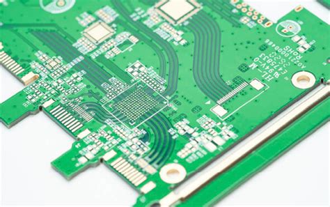
The evolution of PCB fabrication has brought forth High-Density Interconnect (HDI) technology, which plays a pivotal role in modern electronics. As you delve into the world of HDI PCB fabrication, you’ll notice its significance in enhancing device performance while addressing the growing demand for miniaturization. In today’s fast-paced market, PCB manufacturing companies are increasingly adopting HDI techniques, realizing that they offer superior capabilities compared to traditional methods.
One of the driving factors behind this trend is the reduction in PCB manufacturing costs associated with HDI designs. Through optimized layer counts and finer traces, manufacturers can create smaller, more efficient boards that meet stringent functional requirements without compromising on quality. This is especially crucial for industries such as medical devices and aerospace, where reliability and performance are non-negotiable.
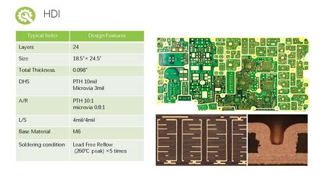
To illustrate, consider a comparison between standard PCBs and those crafted through HDI methods:
| Feature | Standard PCB | HDI PCB |
|---|---|---|
| Layer Count | Up to 4 layers | 6+ layers |
| Trace Width | 10 mils | 3-5 mils |
| Via Size | 0.4 mm diameter | 0.2 mm diameter |
| Electrical Performance | Standard signals | High-speed signals |
As demonstrated in the table above, the advanced capabilities of HDI PCBs pave the way for better functionality in compact designs. Therefore, if you’re involved in a PCB manufacturing business, leveraging these advanced fabrication methods can significantly enhance your competitive edge in an increasingly technology-driven landscape.
Key Technologies Behind HDI Fab Methods
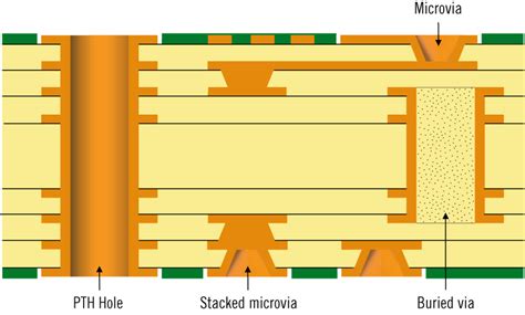
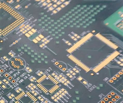
The evolution of High-Density Interconnections (HDI) in PCB manufacturing has significantly advanced the technology behind printed circuit boards. Key technologies driving these methods include laser drilling, which allows for the creation of microvias that facilitate better space utilization and signal integrity. These microvias enable designers to place components closer together, leading to the miniaturization of devices that are vital in industries such as medical equipment and aerospace. Furthermore, employing advanced materials in HDI fabrication enhances thermal management and reliability, addressing critical performance requirements.
IP (Impedance Profile) control is another pivotal technology ensuring that signal integrity is maintained throughout the PCB. By accurately controlling the impedance, manufacturers can minimize noise and reflections, which are of utmost importance in high-frequency applications. Additionally, emerging techniques like electroplating are being utilized for metal filling in blind/buried vias, improving conductivity and overall performance.
When considering your own projects or engaging with various PCB manufacturing companies, it’s important to evaluate not only the pcb manufacturing cost but also how these advanced technologies can ultimately enhance your product’s performance. Investing in high-quality HDI processes ensures that your end devices meet modern standards of efficiency and compactness.
"Always scrutinize the evolving technologies within PCB manufacturing; they could be key to unlocking better performance in your designs."
In summary, advancements in HDI technologies signify a shift towards more sophisticated approaches to PCB design, making it imperative for stakeholders in the pcb manufacturing business to stay informed and adaptable within this rapidly changing landscape.
Advantages of HDI PCBs in Modern Devices
The advantages of HDI PCBs (High-Density Interconnect Printed Circuit Boards) in contemporary devices are profound, fundamentally altering the landscape of pcb manufacturing. By leveraging advanced design techniques and layout efficiency, you can achieve significant miniaturization, which is crucial for today’s compact electronic devices. These benefits are particularly evident in sectors where space and performance are paramount, such as medical equipment and aerospace technology. The pcb manufacturing cost is often offset by the enhanced functionality and reliability that HDI technology brings to the table. With increased electrical performance, including improved signal integrity and reduced power consumption, pcb manufacturing companies can deliver products that meet the rigorous demands of modern applications. Additionally, the agility of HDI technology streamlines the overall pcb manufacturing business, allowing for faster production times and greater flexibility in design iterations. As you explore these advancements, it becomes clear that adopting HDI PCBs not only elevates device capabilities but also supports sustainable practices by enabling more efficient use of materials and resources.
Applications of HDI PCB in Medical Equipment
The use of HDI PCBs in medical equipment plays a pivotal role in advancing healthcare technologies. As you delve into the realm of pcb manufacturing, you will recognize that these high-density interconnects enable the development of smaller, yet more powerful devices that are essential for patient diagnostics and treatment. Medical devices, from imaging equipment to portable patient monitors, require precision and reliability; thus, sourcing from reputable pcb manufacturing companies is crucial. The intricate designs made possible by HDI fabrication help reduce the overall pcb manufacturing cost, allowing manufacturers to allocate resources effectively without compromising on quality. Furthermore, the growth of the pcb manufacturing business is driven by the increasing demand for miniaturized and multifunctional medical devices. By incorporating HDI technology, you can significantly enhance the functionality and portability of medical instruments, ultimately benefiting both healthcare providers and patients alike. The implications of these advancements are profound, as they can lead to improved diagnostics, timely interventions, and better health outcomes across various medical applications.
Impact of HDI Technology on Aerospace Industries
The introduction of High-Density Interconnect (HDI) technology in the aerospace sector marks a significant shift in how aerospace devices are designed and manufactured. As you explore this landscape, you’ll notice that HDI PCBs offer unparalleled advantages over traditional circuit boards, primarily due to their ability to support increased functionality within a smaller footprint. This capability becomes particularly critical when considering the stringent weight and space requirements inherent in aerospace applications. The pcb manufacturing process enables the creation of highly miniaturized components that can endure extreme conditions, such as radiation and vibration. Furthermore, many pcb manufacturing companies are investing heavily in superior fabrication techniques that utilize advanced materials, ensuring not only robustness but also improved thermal management.
The impact on your designs can be profound; with better performance metrics, HDI technology enhances the reliability of critical systems while optimizing performance at a lowered pcb manufacturing cost. This efficiency allows businesses within the aerospace sector to push boundaries further—reducing overall costs while expanding capabilities. As you evaluate opportunities within this realm, understanding how these advancements integrate into your existing workflows could mean the difference between staying relevant and leading in an ever-evolving market. Therefore, embracing HDI technology is not just an option; it’s an imperative for any pcb manufacturing business looking to thrive and innovate passionately within the competitive aerospace arena.
Challenges in HDI PCB Fabrication
The journey of HDI PCB fabrication is not without its hurdles. One of the primary challenges you may encounter is the manufacturing cost, which can be significantly higher than traditional PCB manufacturing techniques. This increased cost often stems from the advanced technologies and materials required to achieve the desired high-density interconnection. Finding reliable PCB manufacturing companies that specialize in these advanced techniques can also pose a challenge. They must possess not only the technical expertise but also the cutting-edge equipment necessary for HDI technology to thrive. Moreover, ensuring quality control throughout the production process is crucial yet intricate, as even minor defects can lead to catastrophic failures in sensitive applications, particularly in sectors such as aerospace and medical devices. As you navigate these obstacles, consider how vital it is to collaborate with reputable partners in your PCB manufacturing business that prioritize precision and quality assurance. The implications of these challenges extend beyond mere fabrication; they influence device performance and ultimately impact your project’s success in fast-paced markets where miniaturization and efficiency are key drivers of advancement.
Future Trends in HDI Technology Developments
As you explore the future trends in HDI PCB fabrication, it’s crucial to consider how innovation will shape the landscape of pcb manufacturing in the coming years. With the ongoing demand for lighter, smaller, and more efficient electronic devices, the need for advanced HDI technology is set to grow exponentially. One of the key developments on the horizon is likely to be enhanced automation in pcb manufacturing companies, which will streamline production processes and reduce human error. Furthermore, evolving design tools and simulation software will enable designers to optimize layouts more effectively, thereby lowering pcb manufacturing costs.
In addition to technological advancements, you may notice a significant push towards sustainability. Many pcb manufacturing businesses are increasingly focusing on eco-friendly materials and processes as environmental concerns take center stage. This shift not only responds to consumer demand but also aligns with global regulations aimed at reducing electronic waste. As you look forward, embracing these trends in HDI PCB fabrication will be essential for staying competitive and meeting market needs across various sectors – from advanced aerospace applications to life-saving medical devices.
Conclusion: The Evolution of PCB Design
The journey of PCB design has reached a pivotal moment with the introduction of advanced HDI PCB fabrication methods. As you explore this evolution, you’ll notice that incorporating high-density interconnects enables designers to achieve unprecedented levels of miniaturization without sacrificing functionality. This evolution not only enhances device performance but also significantly reduces the PCB manufacturing cost, which is a crucial factor for both established firms and emerging startups in the pcb manufacturing business. With the competitive landscape saturating with various pcb manufacturing companies, investing in HDI technology could provide you with an edge over your competitors. The implications for industries like aerospace and medical equipment are vast, as these sectors require devices that are not only robust but also compact and efficient. By adopting advanced fabrication techniques, you can ensure that your projects meet the rigorous demands of modern applications while staying within budget, ultimately leading to a more reliable and efficient manufacturing process. As you reflect on these advancements, consider how they might influence your future designs and drive innovation within your projects.
Conclusion: The Evolution of PCB Design
In the rapidly evolving world of PCB manufacturing, advanced HDI (High-Density Interconnect) techniques have emerged as a groundbreaking solution to meet the intense demands of modern electronics. As you navigate the complexities of this field, it’s crucial to understand how HDI PCB fabrication not only enhances device performance but also significantly reduces the overall size and weight of electronic components. For businesses and professionals within pcb manufacturing companies, this innovation offers a strategic advantage by facilitating more compact designs without compromising functionality.
The reduction in size achieved through these advanced methods directly correlates to lower pcb manufacturing costs, making it an appealing investment for organizations looking to streamline their operations while maintaining high-quality standards. Moreover, as you embrace these pcb manufacturing business advancements, you position your products at the forefront of technology, appealing to industries such as medical and aerospace.
Ultimately, adapting to these changes means not only improving operational efficiency but also opening doors to new markets and applications that demand cutting-edge technology. By keeping updated with such transformative methods in PCB fabrication, your organization can not only stay competitive but also contribute significantly to the future landscape of electronics design.
FAQs
What is HDI PCB fabrication?
HDI PCB fabrication refers to the high-density interconnect printed circuit board manufacturing process which utilizes advanced techniques to produce PCBs with a greater number of connections and smaller features. It significantly contributes to the efficiency and performance of modern electronic devices.
Why should I consider HDI technology for my projects?
You should consider HDI technology because it lightweight and space-efficient design can lead to enhanced device performance. This is particularly crucial in industries where miniaturization is vital, such as in medical equipment and aerospace applications.
What are the benefits of using advanced HDI fabrication methods?
The benefits include improved electrical performance, reduced signal loss, and the ability to integrate more components within a smaller footprint, thus lowering the overall PCB manufacturing cost while enhancing functionality.
Which industries benefit most from HDI PCBs?
Industries such as telecommunications, consumer electronics, medical devices, and aerospace significantly benefit from HDI PCBs due to their need for high-performance and compact electronic solutions.
How does one find reputable PCB manufacturing companies specializing in HDI technology?
You can research online and look for reviews or case studies that highlight companies with a solid reputation in PCB manufacturing, specifically those well-versed in high-density designs. Checking for certifications can also provide insights into their expertise.
What challenges do manufacturers face with HDI PCB fabrication?
Challenges include managing complex designs, higher production costs compared to traditional PCBs, and ensuring quality control during the production process.