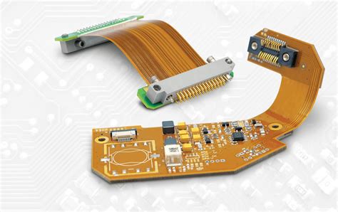
PCB backplane manufacturing technology
The backplane has always been a specialized product in the PCB manufacturing industry. Its design parameters are very different from most other circuit boards. Some stringent requirements need to be met in production. Noise tolerance and signal integrity also require the backplane design to follow unique design rules. These characteristics of the backplane lead to huge differences in its manufacturing requirements such as equipment specifications and equipment processing. In the future, the backplane will be larger and more complex, and will be required to work at unprecedented high clock frequencies and bandwidth ranges. The number of signal lines (tracks) and nodes will continue to increase: it will no longer be uncommon for a backplane to contain more than 50,000 nodes.
1.User needs
Shenzhen Benqiang Circuit (QQ800083129) pointed out that the growing demand of users for increasingly complex large-size backplanes that can work at unprecedented high bandwidths has led to the need for equipment processing capabilities that exceed conventional PCB manufacturing lines. In particular, the backplane is larger, heavier, and thicker, requiring more layers and perforations than standard PCBs. In addition, the required line width and tolerance are more refined, requiring the use of hybrid bus structures and assembly technologies.
2.Requirements for conveying system due to backplane size and weight
The biggest difference between conventional PCB and backplane is the size and weight of the board and the processing of large and heavy raw material substrates (panels). The standard size of PCB manufacturing equipment is typically 24×24 inches. However, users, especially telecommunications users, require larger backplanes. This has promoted the confirmation and purchase of large-size board conveying tools. Designers have to add additional copper layers to solve the routing problem of large-pin connectors, which increases the number of backplane layers. Harsh EMC and impedance conditions also require that the number of layers be increased in the design to ensure adequate shielding, reduce crosstalk, and improve signal integrity.
When a high-power application card is inserted into the backplane, the thickness of the copper layer must be moderate to provide the required current to ensure that the card can work properly. All these factors lead to an increase in the average weight of the backplane, which requires conveyor belts and other conveying systems to not only be able to safely transfer large-size raw material boards, but also to take into account the fact that they are heavier.
The need for thinner cores and more layers of backplanes has created two opposing requirements for the conveying system. The conveyor belt and conveyor must be able to pick up and convey large-format thin sheets less than 0.10mm (0.004 inches) without damage, and must also be able to convey 10mm (0.394 inches) thick, 25 kg (56 pounds) boards without dropping them.
The difference of two orders of magnitude between the thickness of the inner layers (0.1mm, 0.004 inches) and the thickness of the finished backplane (up to 10mm, 0.39 inches) means that the conveying system must be strong enough to safely move them through the processing area. Since the backplane is thicker than a conventional PCB and has many more holes, it is easy to cause the processing fluid to flow out. A large-format 10mm thick backplane with 30,000 holes can easily carry out the small amount of processing fluid adsorbed in the guide holes by surface tension. To minimize the amount of liquid carried and eliminate the possibility of any dried impurities remaining in the guide hole, it is extremely important to clean the drilled hole by high pressure washing and air blower.
3.Layer alignment
As user applications require more and more board layers, the alignment between layers becomes very important. The alignment between layers requires tolerance convergence. The larger the board size, the more stringent this convergence requirement. All layout processes are produced in a certain temperature and humidity controlled environment. The exposure equipment is in the same environment, and the alignment tolerance of the front and back images in the entire area must be maintained at 0.0125mm (0.0005 inches). To achieve this accuracy requirement, a CCD camera is required to complete the alignment of the front and back layouts.
After etching, the inner layer board is perforated using a four-drilling system.
The perforation passes through the core board with a position accuracy of 0.025mm (0.001 inches) and a repeatability of 0.0125mm (0.0005 inches). Then, a pin is inserted into the perforation to align the etched inner layer and bond the inner layer together.
Initially, this post-etch perforation method can fully ensure the alignment of the drilled hole with the etched copper plate, forming a solid ring design structure. However, as users require more and more lines to be laid out in a smaller area in terms of PCB routing, in order to keep the fixed cost of the board unchanged, the size of the etched copper plate is required to be smaller, which requires better alignment of the interlayer copper plate. To achieve this goal, you can use the method of purchasing an X-ray drilling machine. This equipment can achieve a position accuracy of 0.025mm (0.001 inch) for drilling a hole on a board with a maximum size of 1092×813mm (43×32 inches). There are two ways to use it:
- Use an X-ray machine to observe the etched copper on each layer and determine an optimal position with the help of drilling.
- The drilling machine stores statistical data and records the deviation and divergence of the alignment data relative to the theoretical value. Feeding this SPC data back to the previous processing steps such as raw material selection, processing parameters and layout drawing can help reduce its variability and continuously improve the process.
Although the electroplating process is similar to any standard plating process, there are two major differences that must be considered due to the unique characteristics of large-format backplanes.
The fixtures and conveying equipment must be able to transport large-size boards and heavy boards at the same time. The weight of large-format raw material substrates of 1092x813mm (43×32 inches) can reach 25 kg (56 pounds). The substrate must be securely gripped during transportation and processing. The processing tank must be designed to be deep enough to accommodate the board, and uniform electroplating characteristics must be maintained throughout the tank.
In the past, users have specified press-fit connectors for backplanes, thus relying too heavily on the uniformity requirements of copper plating. The backplane thickness produces a variation of 0.8mm to 10.0mm (0.03 inches to 0.394 inches). The existence of various aspect ratios and the increase in substrate specifications make the uniformity of electroplating critical. To achieve the required uniform performance, periodic reverse (“pulse”) electroplating control equipment must be used. In addition, necessary stirring must be performed to keep the electroplating conditions as uniform as possible.
In addition to the requirement for uniform electroplating thickness for drilling, backplane designers generally have different requirements for the uniformity of copper on the outer surface. Some designs etch very few signal lines on the outer layer. On the other hand, facing the needs of high-speed data rates and impedance-controlled lines, it will become necessary to set up nearly solid copper sheets on the outer layer to serve as EMC shielding layers.
4.Detection
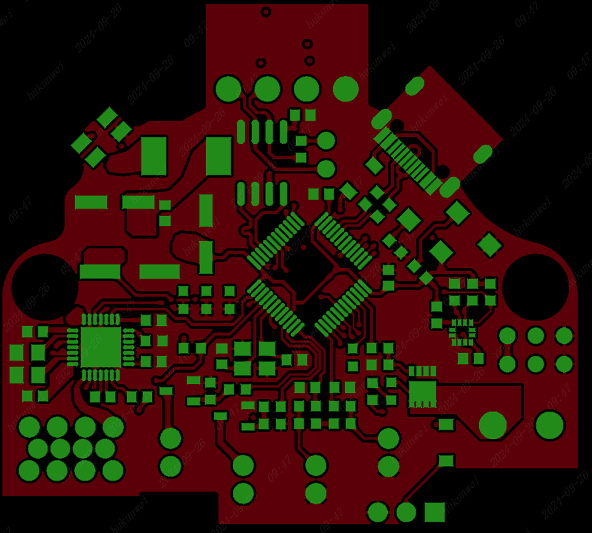
Shenzhen Benqiang Circuit Co., Ltd. (tel: 075529606089) pointed out that since users require more layers, it is very important to ensure that the inner etched layer is defect-identified and isolated before bonding. In order to achieve effective and repeatable control of backplane impedance, etch line width, thickness and tolerance become key indicators. At this time, AOI methods can be used to ensure that the etched copper pattern matches the design data. Using impedance models, the sensitivity of impedance to line width variations is determined and controlled by setting line width tolerances on the AOI.
The trend toward large, multi-drilled backplanes and active circuits on backplanes has combined to promote the need for rigorous inspection of bare boards before component loading for efficient production.
The increase in the number of holes drilled on the backplane means that bare board test fixtures will become very complex, although the use of dedicated fixtures can greatly reduce unit test time. To shorten the production process and prototype manufacturing time, the use of double-sided flying probe fixtures, programmed with original design data, can ensure consistency with user design requirements, reduce costs, and shorten time to market.
5.Assembly
Traditionally, passive components have been preferred on backplanes for reliability reasons. However, in order to maintain fixed costs for active boards, active devices such as BGAs are increasingly designed into backplanes. Component mounting equipment must be able to not only place smaller capacitors and resistors (0402 size), but also be able to operate additional silicon packaged components. In addition, the large size of the backplane requires a large bed for the mounting equipment, and the counterweight backplane can also be shifted with fine position tolerances.
Since the backplane is thicker and heavier than a conventional PCB board, its thermal capacity is correspondingly larger. Since the backplane cools slower, the length of the reflow oven needs to be longer. It also needs to be forced air cooled at the exit to reduce the temperature of the backplane to a level that can be safely operated.