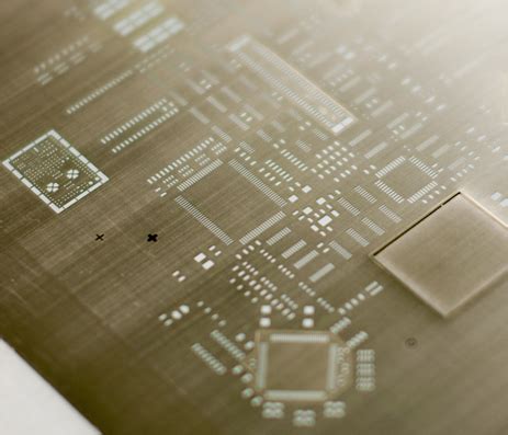
Considerations for designing high-speed circuit boards
Stacking number issues:
A good stacking structure is the best defense against most signal integrity and EMC problems, and it is also the most easily misunderstood. There are several factors at work here, and a good solution to one problem may lead to the exacerbation of other problems.
Many system design vendors will recommend that there should be at least one continuous plane in the circuit board to control characteristic impedance and signal quality, which is good advice as long as the cost can be afforded. EMC consultants often recommend placing ground fill or ground layer on the outer layer to control electromagnetic radiation and sensitivity to electromagnetic interference, which is also good advice under certain conditions. Using capacitor model to analyze signal problems in stacking structure However, due to transient currents, this approach may encounter troubles in some ordinary designs. First, let’s look at the simple case of a pair of power layer/ground layer: it can be regarded as a capacitor. The power layer and ground layer can be considered as the two plates of the capacitor. To get a larger capacitance value, the two plates need to be closer (distance D) and the dielectric constant needs to be increased. The larger the capacitance, the lower the impedance, which is what we want because it can suppress noise. Regardless of how the other layers are arranged, the main power layer and the ground layer should be adjacent and in the middle of the stack. If the power layer and the ground layer are far apart, it will cause a large current loop and bring a lot of noise. If you put the power layer on one side and the ground layer on the other side of an 8-layer board, it will cause the following problems:
- Maximum crosstalk. Due to the increase in mutual capacitance, the crosstalk between the signal layers is greater than the crosstalk of the layers themselves.
- Maximum circulation. The current flows around the power layers and parallel to the signal, and a large amount of current enters the main power layer and returns through the ground layer. EMC characteristics will deteriorate due to the increase in circulation.
- Loss of control of impedance. The farther the signal is from the control layer, the lower the accuracy of impedance control due to other conductors around it.
- Due to the easy solder short circuit, it may increase the cost of the product.

Characteristic impedance: We must make a compromise between performance and cost. To this end, I would like to share my views on how to arrange digital circuit boards to obtain the best SI and EMC characteristics. The distribution of each layer of the PCB is generally symmetrical. In my humble opinion, more than two signal layers should not be placed adjacent to each other; otherwise, SI control will be lost to a large extent. It is best to place the internal signal layers symmetrically in pairs.
Unless some signals need to be connected to SMT devices, we should minimize the signal wiring on the outer layer. The first step of an excellent design is to correctly design the stacking structure. For circuit boards with more layers, we can repeat this placement method many times. Additional power layers and ground layers can also be added; as long as there is no paired signal layer between the two power layers. The routing of high-speed signals should be arranged in the same pair of signal layers; unless this principle has to be violated due to the connection of SMT devices. All traces of a signal should have a common return path (i.e., ground layer). There are two ideas and methods to determine what kind of two layers can be considered a pair: 1. Ensure that the return signals at equal distances are completely equal. That is to say, the signal should be routed symmetrically on both sides of the internal ground layer. The advantage of this is that it is easy to control impedance and circulation; the disadvantage is that there are many vias on the ground layer and some useless layers.
- Two signal layers with adjacent wiring. The advantage is that the vias in the ground layer can be controlled to a minimum (using buried vias); the disadvantage is that the effectiveness of this method is reduced for some critical signals.
I like to use the second method. The ground connection of the component driving and receiving signals is best connected directly to the layer adjacent to the signal wiring layer. As a simple wiring principle, the surface wiring width in inches should be less than one-third of the driver rise time in milliseconds (for example: the wiring width of high-speed TTL is 1 inch). If multiple power supplies are used, ground layers must be laid between the metal wires of each power supply to separate them. No capacitance can be formed to avoid AC coupling between power supplies. The above measures are all to reduce circulation and crosstalk and enhance impedance control capabilities.
The ground layer will also form an effective EMC “shielding box”. Under the premise of considering the impact on the characteristic impedance, unused surface areas can be made into ground layers. Characteristic Impedance A good stackup structure will effectively control impedance, and its traces will form a well-understood and predictable transmission line structure. Field Solver handles this type of problem very well, and as long as the number of variables is kept to a minimum, you can get fairly accurate results.
However, this is not necessarily the case when more than three signal layers are stacked together, and the reason is subtle.
The target impedance value depends on the process technology of the device. High-speed CMOS technology generally achieves about 70 Ω; high-speed TTL devices generally achieve about 80 Ω to 100 Ω.
Because the impedance value usually has a great impact on noise margins and signal switching, impedance selection needs to be very careful; the product manual should provide guidance on this. The initial results of the Field Solver may encounter two problems. The first is the problem of limited field of view. The Field Solver only analyzes the impact of nearby traces, and does not consider non-parallel traces on other layers that affect impedance. The Field Solver cannot know the details before routing, that is, when assigning trace widths, but the above pair arrangement method can minimize this problem.
It is worth mentioning the impact of partial power planes.
Outer layers are often packed with ground copper after routing, which helps suppress EMI and balance plating. If only the outer layers are taken, the stackup structure recommended in this article will have little effect on characteristic impedance. The effect of using a large number of adjacent signal layers is very significant. Some field solution tools cannot detect the presence of copper foil because they can only check the traces and the entire layer, so the impedance analysis result is incorrect
When there is metal on the adjacent layer, it acts like an unreliable ground layer.
If the impedance is too low, the instantaneous current will be large, which is a real and sensitive EMI problem. Another reason for the failure of impedance analysis tools is distributed capacitance. These analysis tools generally do not reflect the effect of pins and vias (this effect is usually analyzed with simulators). This effect can be large, especially on backplanes. The reason is very simple: the characteristic impedance can usually be calculated as follows: √L/C where L and C are the inductance and capacitance per unit length, respectively.
If the pins are arranged evenly, the additional capacitance will greatly affect this calculation result. The formula becomes: √L/(C+C’) C’ is the pin capacitance per unit length. If the connectors are connected by straight lines, as on a backplane, the total line capacitance and the total pin capacitance except for the first and last pins can be used. In this way, the effective impedance will be reduced, perhaps even from 80 Ω to 8 Ω. To get the effective value, divide the original impedance value by: √(1+C’/C) This calculation is important for component selection. When simulating delays, the capacitance of the component and package (and sometimes the inductance) should be considered. There are two issues to be aware of.
First, the simulator may not be able to correctly simulate distributed capacitance;
second, be aware of the impact of different production conditions on incomplete layers and non-parallel traces. Many field solution tools cannot analyze stackup distributions without full power or ground layers. However, if there is a ground layer adjacent to the signal layer, the calculated delay will be quite bad, such as capacitance, which will have the maximum delay; this is even more serious if both layers of a double-sided board are covered with many ground and VCC copper foils. Setting these things up in a CAD system can be very messy if the process is not automated. EMC There are many factors that affect EMC, many of which are usually not analyzed. Even if they are analyzed, it is often too late after the design is completed. Here are some factors that affect EMC:
- The slots in the power layer will form a quarter-wavelength antenna. For situations where mounting slots are required on metal containers, drilling methods should be used instead.
- Inductive components. I once met a designer who followed all the design rules and did simulations, but his circuit board still had a lot of radiated signals. The reason is: there are two inductors placed parallel to each other on the top layer, forming a transformer.
- Due to the influence of the incomplete ground layer, the low impedance of the inner layer causes a large transient current in the outer layer. Most of these problems can be avoided by using defensive design. First, the correct stacking structure and wiring strategy should be made, so that you have a good start. Some basic issues, such as network topology, signal distortion causes and crosstalk calculation methods, are not involved here; only some sensitive issues are analyzed to help readers apply the results obtained from the EDA system. Any analysis depends on the model used, and factors that cannot be analyzed will also affect the results. Too much complexity is like too much imprecision. Avoiding too many changes in parameters, such as trace width, contributes to a neat and consistent design.