Innovative FPGA Technology Enables Low-Power, Modular, Small-Size USB Solutions
Innovative FPGA Technology Enables Low-Power, Modular, Small-Size USB Solutions
USB technology development faces unique challenges, mainly due to the need to achieve robust interconnect, high speed, and power management within a constrained device form factor. Various device compatibility issues, varying data transfer speeds, and requirements for low latency and low power consumption put additional pressure on engineers to innovate within tight technology constraints. Engineers must integrate USB functionality into increasingly smaller modules and balance functionality with design constraints.
This article summarizes some of the typical solutions used in the industry for high-performance USB 3 devices and introduces a new architecture that saves power and area while increasing flexibility and ease of use.
Lattice recently released a new FPGA family with native USB 3.2 Gen 1, called Lattice CrossLinkU-NX. In addition to the product datasheet, this article will also provide a detailed introduction to the device. Some of the standout features of the CrossLinkU-NX device are as follows:
- Integrated USB 2.0 and 3.2 support, providing data transfer speeds up to 5 Gbps
- Higher integration significantly reduces board design size and power consumption
- Supports a wide range of interfaces (MIPI, LVDS, CMOS) and advanced security features (AES256 and ECC256)
- Provides low-power standby and versatile DSP resources to optimize AI performance
- Ideal for industrial, automotive, and consumer applications
Over the past few years, tinyVision.ai has worked closely with Lattice Semiconductor to develop a complete USB solution that integrates advanced FPGA technology with modular, high-performance USB functionality. This collaboration enables tinyVision to leverage Lattice’s CrossLinkU-NX FPGA platform to drive efficiency, scalability, and flexibility in USB design. This complete solution, including hardware, RTL, and firmware, is very helpful to customers, who can modify it according to their requirements in addition to referring to the application notes.
By combining tinyVision’s strengths in firmware and modular hardware design with Lattice’s cutting-edge FPGA capabilities, this collaboration has resulted in an innovative solution that redefines USB interconnect for modern embedded systems and multimedia applications.
Today’s industrial cameras require efficient bridging capabilities
Today, low-speed or high-speed USB solutions are common in many devices with limited bandwidth requirements and are also widely used in many low-end microcontrollers. However, USB SuperSpeed is required for applications such as industrial cameras, software-defined radios, etc.
FPGAs are often used as signal acquisition and processing front ends in a wide range of applications such as industrial cameras, handheld ultrasound, logic analyzers, and software-defined radios. To communicate with USB 3, FPGAs are often connected to USB bridge chips.
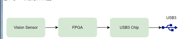
Figure 1. A typical USB3 peripheral using an FPGA and USB3 bridge chip
The interface between the FPGA and the bridge chip is usually a parallel FIFO interface. Bridge chips are simple data pumps and have no access to the data stream itself. They are usually able to add headers/footers to meet protocol requirements. The signal processing tasks for the various camera-related functions (such as AEC, AGC, AWB, gamma, lens correction, etc.) required by the ISP (Image Signal Processor) are handled by the FPGA.
CrossLinkU-NX FPGA: A Device that Revolutionizes USB Design
The significance of CrossLinkU-NX is that it combines two chips that are usually paired together: FPGA and USB 3 interface into a single device.
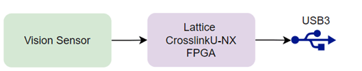
Figure 2. Improved system architecture using Lattice CrossLinkU-NX device
Compared with other similar USB 3 bridge solutions on the market, its advantages are smaller footprint, lower power consumption, lower BoM cost, lower manufacturing cost, and only one tool chain to master and manage. The line rate of the UVC layer is 5 Gbps, and the measured throughput is 3.4 Gbps, which provides sufficient bandwidth for high resolution, high frame rate and multi-camera systems.
Architecturally, the data FIFO can be pulled into the FPGA. This flexible architecture enables potential new applications that were not possible before (for example, USB endpoints can now be assigned to various peripherals under the control of the designer instead of a limited number dictated by the chip vendor). This makes it easy to support multiple camera streams, for example.
In addition, board design is greatly simplified due to the significantly reduced number of components (and fewer supply chain issues), and the direct sensor interface, which eliminates the need for numerous FIFO lines on the board and the need for inter-chip control signals.
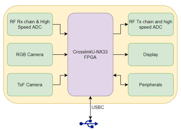
Figure 3. Conceptual block diagram of a USB device based on CrossLinkU-NX FPGA
tinyVision.ai’s innovative approach
tinyVision’s solution consists of the following:
- SoM (System on Module) for rapid prototyping and production-ready
- Streamlined RTL built around USB hard core IP to maximize USB bandwidth and efficiency
- Zephyr RTOS driver for the IP to simplify complex USB protocols
- Tool flows and complete reference designs provide a good starting point for developers
- Design services from driver development to full product development to support customers
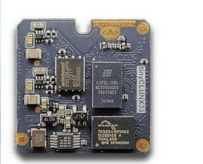
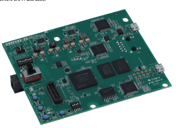
Figure 4. tinyVision.ai tinyCLUNX33 SoM MIPI-UVC converter
The modular hardware and firmware architecture enables interchangeable components, allowing teams to add USB functionality to their products with minimal effort.
The SoM hardware supports USB 3.2 Gen1, ensuring high-speed data and low power consumption for designs with limited size. Due to the Syzygy standard, a variety of adapter boards can be used to enable rapid prototyping.
On top of the Zephyr RTOS, tinyVision has developed a “USB as an API” approach that implements a zero-configuration USB API that automatically generates compliant USB descriptors. This allows for seamless USB integration, allowing developers to handle USB calls like any other API request. In addition to this significant simplification, tinyVision has been committed to open source development, including continuous optimization of its USB 3 drivers in open source projects and active participation in the development of Zephyr’s UVC (USB Video Class) driver, which is very important for video streaming.
The SoM is supported by a rich suite of IPs, including USB IPs and SRAM controllers, which have been tested on the platform to simplify integration.
tinyVisional also provides a suite of image and audio processing IPs using StreamLogic technology. This suite of IPs supports low-latency stream processing, ideal for real-time applications such as video streaming and audio playback, enabling advanced multimedia capabilities in USB devices.
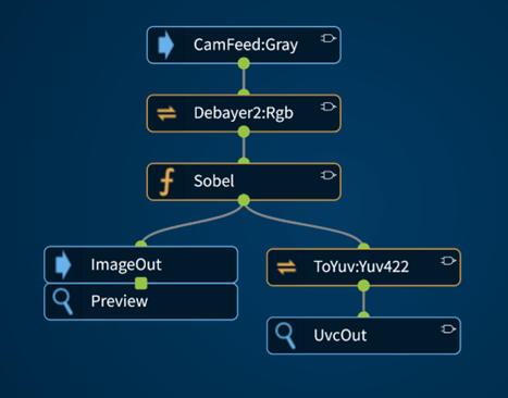
Figure 5. Example of a complete image processing pipeline using Streamlogic’s code-free graphical design tool. Audio and neural network IPs are also available.
7 Advantages of the New USB Device Architecture
- Lower power consumption compared to typical FPGA + dedicated USB3 FIFO chips.
- USB 3 bandwidth + high-performance signal processing: The USB solution can effectively utilize the full bandwidth of the USB3 physical layer and provide a sustained data rate of 3.4Gbps at the UVC layer. FPGAs also have a large amount of on-chip computing resources, which can not only implement ISP, but also advanced functions such as object detection/tracking.
- Small size: The use of a micro CSP package of 3.1 mm x 7.4 mm enables ultra-small device size.
- Programmable flexibility: The data flow architecture of traditional FPGA + bridge chips is very limited. By integrating the USB core in the FPGA architecture, more data paths can be realized.
- Powerful firmware and IP support: tinyVision’s Zephyr port provides users with an industrial-grade modern RTOS, which has a large open source driver library and a broad and helpful community. StreamLogic technology and MIPI-UVC and SRAM controller IP can help rapid development.
- Enhanced security features: Bit file encryption and other industry-leading security features ensure customer designs are secure.
- Faster time to market: The SoM approach allows for faster time to market, as the most complex parts of the design have already been verified with the RTL and Zephyr reference designs.
Customers using low-power, modular, small-footprint solutions
Constructive Realities is in the business of digitizing and organizing spatial data. They are developing a custom 3D vision system that includes a co-located Time of Flight (ToF) and RGB camera, as well as spatial tracking and reconstruction running on a small ARM SBC. The solution requires small size, battery power, and low cost.
ToF processing is very complex and requires a lot of memory bandwidth and compute power from the host, so the application processor needs to handle all aspects of the vision pipeline. The default solution is to use an FPGA to manage the RGB and ToF sensors and data processing, and use a FIFO-USB 3 chip (such as chipsets from Cypress or FTDI) to stream the data over USB to the end user.
Power savings and significant reduction in BoM complexity by eliminating the FTDI/Cypress bridge chip and its supporting circuitry (bridge chip, memory, power supply and other passives).
The tinyVision UVC solution provides flexibility that accelerates development efforts by sending raw MIPI data from both sensors directly to the host where the original algorithm is developed. Our customer then ported the computationally expensive ToF algorithm to the SoM, using off-the-shelf parts to reduce the computational requirements on the connected system.
Zephyr is a key part of the solution due to its modularity, small footprint and strong community support. The SoM will be part of their final product with minimal investment in developing an add-in card that hosts the SoM, power supply, IMU and 2 image sensors.
Enable reliable, efficient and secure USB connectivity
The collaboration between tinyVision and Lattice Semiconductor has resulted in a revolutionary USB device solution with CrossLinkU-NX FPGA at its core. It combines USB 3.2, advanced FPGA capabilities and comprehensive firmware support provided by Zephyr RTOS to deliver a small form factor, low power and highly flexible platform.
This solution greatly simplifies the development of USB devices while reducing costs and time to market, making it ideal for a variety of applications such as industrial cameras and medical equipment. These applications benefit from the flexibility, scalability and high performance of this solution to achieve reliable, efficient and secure USB connections in mission-critical systems.
Whether it is used for real-time data processing, multimedia or embedded systems, tinyVision’s technology can support the complex requirements of these different fields.
These revolutionary USB solutions from tinyVision will be demonstrated at the Lattice 2024 Developer Conference held on December 10-11. By registering to participate in the Lattice Developer Conference, you will have the opportunity to learn from experienced FPGA experts and experience more than 75 innovative technology demonstrations from partners from multiple industries.