Essential Steps in Through Hole PCB Assembly
Key Takeaways
Effective through-hole PCB assembly relies on meticulous attention to several core processes. First, component insertion demands precise alignment of leads with designated holes on the PCB, ensuring proper orientation and fit. This step is critical for avoiding misalignment during soldering. Next, soldering techniques, such as wave soldering or manual soldering, must be selected based on component density and thermal requirements to create durable electrical connections.
Quality assurance is integral to PCBA success. Post-soldering, inspection methods like automated optical inspection (AOI) or X-ray analysis help identify defects such as cold joints or insufficient solder fill. Additionally, functional verification through electrical testing ensures the assembled board meets performance specifications.
Below is a comparison of common soldering methods:
| Technique | Process | Pros | Cons |
|---|---|---|---|
| Wave Soldering | PCB passed over molten solder wave | High speed, consistent results | Limited to single-side assembly |
| Manual Soldering | Hand-applied with iron | Precision for rework or prototypes | Labor-intensive, variable quality |
Key challenges in through-hole PCB assembly include managing thermal stress during soldering and avoiding tombstoning of components. Adhering to industry standards like IPC-A-610 ensures reliability. By integrating robust PCB assembly practices—such as proper flux application and controlled cooling—manufacturers can enhance the longevity and functionality of the final PCBA.
Introduction to Through-Hole Technology in PCB Assembly
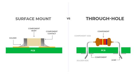
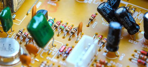
Through-hole technology (THT) remains a foundational method in PCB assembly (PCBA) for applications requiring robust mechanical bonds and high reliability. Unlike surface-mount technology (SMT), which dominates modern miniaturized electronics, THT involves inserting component leads through pre-drilled holes in the printed circuit board (PCB), followed by soldering to create permanent connections. This approach is particularly advantageous for components subjected to mechanical stress, high power, or thermal fluctuations, such as connectors, transformers, and large capacitors. The durability of through-hole connections makes them a preferred choice in industries like automotive, aerospace, and industrial equipment, where long-term performance under demanding conditions is critical.
The PCB assembly process for through-hole components begins with precise hole alignment and component insertion, ensuring leads pass smoothly through the board. Manual or automated insertion methods may be employed, depending on production scale and complexity. Once components are seated, soldering—typically via wave soldering or hand soldering—secures the leads to copper pads, forming both electrical and mechanical bonds. Proper soldering techniques are vital to avoid defects like cold joints or bridging, which can compromise functionality. Post-soldering, rigorous inspection (visual or automated optical inspection) verifies joint quality and component placement accuracy. By integrating THT into PCBA workflows, manufacturers balance the need for durability with the flexibility to support mixed-technology boards that combine through-hole and surface-mount components.
Preparing the PCB for Component Insertion
Before initiating through-hole PCB assembly, thorough preparation of the printed circuit board (PCB) ensures seamless component integration and long-term reliability. The first step involves cleaning the board to remove contaminants such as dust, oils, or residues from manufacturing. Even minor impurities can hinder solder adhesion or cause electrical shorts during PCBA.
Next, inspect the PCB for physical defects, including cracks, misaligned drill holes, or damaged copper traces. Tools like magnifying lenses or automated optical inspection (AOI) systems help identify imperfections that might compromise PCB assembly quality. Pre-cleaning and inspection are critical, as undetected flaws at this stage may lead to costly rework later.
After verification, apply solder paste or flux to the through-holes. While solder paste is common in surface-mount technology (SMT), flux is often preferred in through-hole PCB assembly to enhance wetting and prevent oxidation during soldering. A thin, even coating ensures optimal solder flow and strong mechanical bonds.
Tip: Use a flux applicator or stencil to control the amount applied, avoiding excess that could cause bridging or residue buildup.
Organize components according to the Bill of Materials (BOM) and verify their specifications (e.g., lead length, polarity). Pre-bend component leads slightly to align with hole spacing, reducing insertion force and stress on the PCB. For high-density boards, label components or group them by placement order to streamline the PCBA process.
Finally, ensure the work environment is static-free and temperature-controlled. Moisture-sensitive components should be stored in dry cabinets, and anti-static mats or wrist straps must be used to prevent electrostatic discharge (ESD) damage. Proper preparation minimizes assembly errors and lays the foundation for efficient soldering and inspection phases.
Step-by-Step Component Placement and Alignment
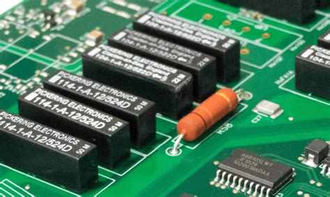
Effective PCB assembly relies on precise component placement and alignment, particularly in through-hole technology (THT). The process begins by inserting components into pre-drilled holes on the board, ensuring leads protrude through the opposite side. For accuracy, technicians often reference the bill of materials (BOM) and assembly drawings to verify component orientation, polarity, and positioning. Axial components (e.g., resistors, diodes) and radial components (e.g., capacitors, connectors) require distinct handling—axial parts are inserted horizontally, while radial parts align vertically.
Manual insertion is common for low-volume PCBA projects, where operators use tweezers or specialized tools to place components. For high-volume production, automated insertion machines streamline the process, minimizing human error. Regardless of the method, proper lead bending or clinching—a technique where leads are slightly bent post-insertion—ensures components remain secure during soldering. Misaligned parts can lead to poor solder joint integrity or electrical shorts, underscoring the need for meticulous inspection before moving to the next stage.
Alignment tools, such as custom jigs or optical alignment systems, further enhance precision, especially for complex boards with dense layouts. Critical components like connectors or switches often require additional verification to match mechanical specifications. Once all parts are correctly positioned, the board is ready for soldering, where proper alignment directly impacts the reliability and durability of the final product. This phase bridges design intent with functional reality, making it a cornerstone of successful through-hole PCB assembly.
Soldering Techniques for Through-Hole Components
Effective soldering is critical to ensuring robust electrical and mechanical connections in through hole PCB assembly. Two primary methods dominate this stage: manual soldering and wave soldering. For low-volume or prototype PCBA, manual soldering with a soldering iron is common. Operators must carefully control temperature (typically 300–350°C) to avoid thermal damage while ensuring adequate solder flow into plated through-holes. A 60/40 or 63/37 tin-lead alloy—or lead-free alternatives like SAC305—is applied to form a concave fillet around the component lead and pad, indicating a proper bond.
For high-volume production, wave soldering streamlines the process. Boards pass over a molten solder wave, which contacts the underside, wicking upward through holes to create connections. Key parameters include conveyor speed, solder temperature (~250–265°C for lead-free), and flux application. Proper flux activation removes oxides and enhances wetting, while preheating prevents thermal shock. After soldering, residual flux is cleaned using solvents or aqueous solutions to prevent corrosion.
Inspection is vital. Visual checks identify issues like cold joints, bridging, or insufficient fill. Automated optical inspection (AOI) systems may scan for defects, while cross-sectional analysis verifies hole penetration. For mission-critical PCB assembly, X-ray inspection ensures internal voids or cracks are absent. By adhering to these techniques, manufacturers achieve reliable PCBA with durable through-hole connections, essential for applications demanding mechanical stability or high-power handling.
Inspection and Quality Control in Assembly
Thorough inspection and quality control are critical to ensuring the reliability of through-hole PCB assembly. After components are inserted and soldered, the PCBA undergoes rigorous checks to identify defects such as misaligned pins, insufficient solder joints, or cold joints. Visual inspection, often performed manually or with automated optical inspection (AOI) systems, verifies component placement accuracy and solder fillet quality. For high-volume production, AOI tools use cameras and algorithms to detect deviations from design specifications, flagging issues like tombstoning or bridging.
Electrical testing, such as in-circuit testing (ICT), may also be integrated into the PCB assembly process to validate connectivity and functionality. This step ensures that each through-hole component—resistors, capacitors, connectors—operates within its specified parameters. Additionally, mechanical stress tests assess solder joint durability, simulating real-world conditions to prevent failures in demanding environments.
Quality control protocols in PCBA emphasize adherence to industry standards like IPC-A-610, which defines acceptability criteria for soldered connections. Inspectors check for proper wetting, fillet shape, and the absence of voids or cracks. Defective boards are reworked or discarded to maintain consistency across batches. By combining automated systems with human expertise, manufacturers minimize errors and deliver durable, high-performance circuit boards that meet both technical and regulatory requirements.
Common Challenges in Through-Hole PCB Assembly
While through-hole PCB assembly offers durability and mechanical stability, it presents several challenges that require careful attention. One common issue is component misalignment during insertion, particularly with densely populated boards or multi-pin parts like connectors. Even minor deviations can lead to poor electrical connections or mechanical stress. Another challenge involves soldering defects, such as cold joints or solder bridging, which may occur due to inconsistent heat application or insufficient flux activity. These defects compromise the reliability of the PCBA and often necessitate rework.
Thermal management is another critical concern, as excessive heat during wave soldering can damage sensitive components or warp the board. Conversely, insufficient heat results in incomplete solder fillets, weakening the bond. Additionally, manual inspection of through-hole joints can be time-consuming, especially for boards with complex layouts, as hidden solder connections under components may escape visual detection. Automated optical inspection (AOI) systems help but may struggle with three-dimensional through-hole structures.
Environmental factors, such as humidity, can also affect component leads, leading to oxidation that hinders solderability. Pre-assembly storage conditions and proper handling of moisture-sensitive components are vital to mitigate this risk. Finally, balancing cost and efficiency remains a hurdle, as through-hole PCB assembly often requires more labor and material compared to surface-mount alternatives. Addressing these challenges demands a combination of precise process control, skilled workforce training, and advanced inspection tools to ensure robust and reliable PCBA outcomes.
Best Practices for Reliable Through-Hole Connections
Achieving robust through-hole PCB assembly requires adherence to proven methodologies that prioritize precision and consistency. A critical first step is ensuring proper component insertion, where leads must align seamlessly with plated holes. Components should be inserted flush against the board to avoid misalignment, which can compromise electrical connectivity during PCBA processes. For manual assembly, tools like insertion guides or fixtures help maintain accuracy, while automated systems rely on programmable placement equipment to achieve repeatability.
Soldering is the cornerstone of durable through-hole connections. Wave soldering remains a widely used technique in PCB assembly, particularly for high-volume production. Here, the board passes over a molten solder wave, creating uniform fillets around component leads. For low-volume or rework scenarios, hand soldering with a temperature-controlled iron is preferred, though it demands skilled operators to prevent cold joints or overheating. Regardless of the method, solder alloy selection—typically lead-free SAC305 or Sn63/Pb37—plays a vital role in joint integrity and thermal resilience.
Post-soldering inspection is non-negotiable. Visual checks under magnification identify issues like insufficient wetting, bridging, or voids. Automated optical inspection (AOI) systems enhance efficiency by scanning for defects at scale, while X-ray imaging verifies hidden connections in multi-layer boards. Stress testing, including thermal cycling and vibration assessments, further validates reliability under real-world conditions.
To mitigate common challenges such as tombstoning or pad lifting, ensure adequate hole-to-lead ratios and avoid excessive mechanical force during insertion. Additionally, pre-tinning component leads and using flux tailored for PCBA applications improve solder flow and adhesion. Finally, maintaining a clean workspace free from contaminants like dust or moisture prevents oxidation and ensures consistent performance. By integrating these practices, manufacturers can deliver through-hole assemblies that meet stringent quality standards and endure demanding operational environments.
Final Testing and Functional Verification
The ## Final Testing and Functional Verification phase is critical to ensuring the reliability and performance of a through-hole PCB assembly. After components are securely soldered and inspected, the assembled board (PCBA) undergoes rigorous testing to validate its functionality under real-world conditions. Functional testing typically involves powering up the board and simulating operational scenarios to verify that all circuits, connections, and components behave as intended. Automated test equipment (ATE) or custom test jigs may be used to apply input signals and measure outputs, checking for anomalies like short circuits, open connections, or incorrect voltage levels.
In parallel, in-circuit testing (ICT) probes individual components to confirm proper placement, orientation, and soldering integrity. For high-reliability applications, environmental stress testing—such as thermal cycling or vibration tests—might be conducted to assess durability under extreme conditions. Visual inspections using magnification tools or automated optical inspection (AOI) systems are also repeated to catch any latent defects missed earlier.
Documentation of test results is essential, providing traceability and compliance with industry standards. Any failures detected during this phase require root-cause analysis and rework before the PCB assembly is approved for deployment. By combining automated and manual verification methods, manufacturers ensure that every through-hole PCBA meets design specifications and delivers consistent, long-term performance.
Conclusion
In PCB assembly, the through-hole method remains a cornerstone for creating robust electronic circuits, particularly where mechanical stability and durability are paramount. The process hinges on meticulous execution of key steps: component insertion, soldering, and inspection. Proper alignment of components during insertion ensures that leads fit seamlessly into designated holes, minimizing the risk of misconnections or physical stress. During soldering, techniques such as wave soldering or hand soldering must be carefully applied to achieve consistent solder joints without causing thermal damage to the board or components. Post-soldering inspection—encompassing automated optical inspection (AOI) and X-ray analysis—is critical for identifying defects like cold joints, bridging, or incomplete fills. Challenges such as component spacing conflicts or solder wicking can arise, but adherence to industry standards and best practices mitigates these risks. Final functional testing validates the PCBA‘s performance under real-world conditions, ensuring reliability. By integrating precision at every stage, manufacturers can deliver through-hole assemblies that meet stringent quality benchmarks, underscoring the method’s enduring relevance in modern electronics.
FAQs
What is the primary difference between through-hole and surface-mount PCB assembly?
Through-hole PCB assembly involves inserting component leads into pre-drilled holes on the board, while surface-mount technology (SMT) places components directly onto the board’s surface. PCBA using through-hole offers stronger mechanical bonds, ideal for high-stress environments.
How crucial is component alignment in through-hole PCB assembly?
Proper alignment ensures leads fit seamlessly into holes, preventing soldering defects. Misaligned components can cause short circuits or PCB assembly failures during testing. Automated insertion tools or manual checks are often used for precision.
What soldering techniques are recommended for through-hole components?
Wave soldering is common for high-volume PCBA, where the board passes over a molten solder wave. Hand soldering suits prototypes or repairs. Both methods require controlled temperatures to avoid thermal damage to components.
Why is inspection critical after through-hole PCB assembly?
Inspection identifies issues like cold joints, incomplete solder fill, or misplaced components. Automated optical inspection (AOI) and manual checks ensure reliability before proceeding to final testing.
What are common challenges in through-hole assembly?
Component lead bending, hole size mismatches, and solder bridging are frequent issues. Implementing design-for-manufacturing (DFM) principles and rigorous quality control minimizes these risks.
How can through-hole connections be made more reliable?
Use high-quality solder, maintain clean boards, and ensure proper hole-to-lead ratios. Conformal coating adds protection against environmental factors in finished PCBA units.
What tests validate through-hole PCB functionality?
Functional testing, in-circuit testing (ICT), and environmental stress screening (ESS) verify performance under real-world conditions. These steps ensure the PCB assembly meets design specifications.
Ready to Optimize Your Through-Hole PCB Assembly Process?
For expert guidance and tailored solutions in PCB assembly, please click here to explore our services and enhance your project’s reliability.