Optimizing SMT PCB Assembly for High-Quality Electronics Production
Key Takeaways
Optimizing SMT PCB assembly processes is critical for achieving high-quality electronics manufacturing. Key strategies include prioritizing component placement accuracy through precision machinery and real-time calibration, which minimizes misalignment and solder defects. Advanced solder paste application techniques, such as laser-cut stencils and automated jet dispensing, ensure uniform deposition, reducing voids and bridging. Thermal profiling during reflow soldering must account for board complexity and component density to maintain consistent heat distribution, preventing cold joints or component damage.
Integrating Automated Optical Inspection (AOI) systems enables rapid detection of flaws like solder skips or misplaced components, significantly lowering defect rates in PCBA workflows. Material selection plays a pivotal role—using high-grade solder paste, moisture-sensitive component storage, and standardized PCB substrates enhances reliability. Smart process integration, including IoT-enabled monitoring and predictive maintenance, streamlines production while reducing downtime.
| Optimization Strategy | Key Benefit | Impact on Quality |
|---|---|---|
| Precision Component Placement | Reduces misalignment risks | Improves electrical connectivity |
| Advanced Solder Paste Techniques | Minimizes voids and bridging | Enhances solder joint integrity |
| AOI Implementation | Identifies defects early in production | Lowers rework costs and improves yield |
Lastly, rigorous quality control protocols, such as cross-functional testing and failure mode analysis, ensure long-term reliability. By aligning these practices, manufacturers can achieve superior PCB assembly outcomes with fewer defects and higher performance consistency.
Understanding the Fundamentals of SMT PCB Assembly
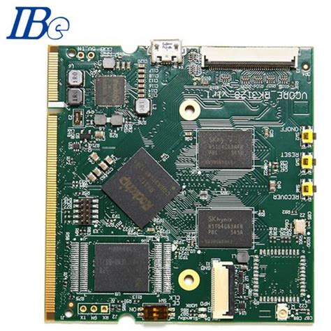
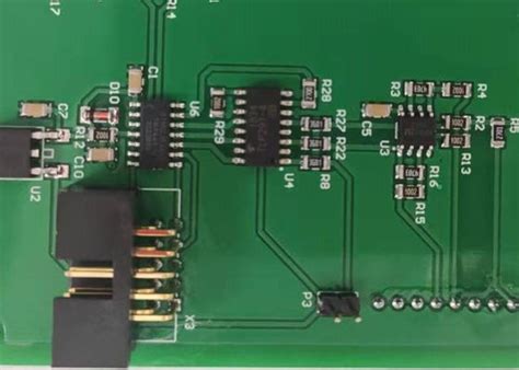
SMT (Surface Mount Technology) PCB assembly forms the backbone of modern electronics manufacturing, enabling the precise placement of miniature components onto printed circuit boards. Unlike traditional through-hole methods, SMT PCB assembly relies on mounting components directly onto the board’s surface, optimizing space utilization and improving electrical performance. This process is central to PCBA (Printed Circuit Board Assembly), where accuracy in component placement, solder application, and thermal management directly impacts product reliability and functionality.
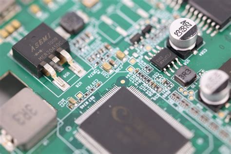
A critical aspect of SMT PCB assembly is the use of pick-and-place machines, which automate the positioning of surface-mount devices (SMDs) with micron-level precision. These machines work in tandem with solder paste stencils, which apply a controlled layer of solder paste to designated pads, ensuring consistent electrical connections during reflow soldering. The interplay between stencil design, solder paste viscosity, and component orientation dictates the success of the PCBA process, minimizing defects such as bridging or tombstoning.
Equally vital is the role of thermal profiling in reflow ovens, which ensures solder joints achieve optimal metallurgical bonds without damaging sensitive components. By carefully calibrating temperature zones, manufacturers avoid issues like cold joints or component warping, which are common pitfalls in high-density PCB assembly. Additionally, material selection—such as choosing high-quality substrates and solder alloys—enhances the durability and thermal resilience of the final PCBA, particularly in demanding environments.
Understanding these fundamentals underscores the importance of integrating advanced inspection systems, such as Automated Optical Inspection (AOI), to validate placement accuracy and solder quality at early stages. This proactive approach reduces rework costs and ensures compliance with industry standards. By mastering the core principles of SMT PCB assembly, manufacturers lay the groundwork for scalable, high-yield production of sophisticated electronic devices.
Key Strategies for Optimizing Component Placement Accuracy
Achieving precision in component placement is critical for ensuring the functionality and reliability of SMT PCB assembly processes. Modern PCBA workflows rely heavily on automated pick-and-place systems, which must balance speed with meticulous accuracy. To optimize placement accuracy, manufacturers should prioritize calibration of machinery, leveraging advanced vision systems to align components within micron-level tolerances. High-speed cameras and laser-guided alignment tools can detect subtle deviations in PCB pad geometries, correcting placement errors before soldering.
A key strategy involves optimizing the stencil design to match component footprints, ensuring proper solder paste deposition. This reduces misalignment risks during placement. Additionally, employing dynamic nozzle systems that adapt to varying component sizes and shapes enhances flexibility without compromising speed. For ultra-fine-pitch components, such as micro-BGAs or 0201 passives, vacuum-controlled placement heads minimize positional shifts caused by vibration or airflow.
Tip: Regularly validate placement accuracy using sample boards with fiducial markers. This helps verify machine calibration and identifies drift in real-world conditions.
Material handling also plays a role. Moisture-sensitive components should be stored in controlled environments to prevent warping, which can skew placement. Integrating AOI (Automated Optical Inspection) systems post-placement provides immediate feedback, flagging misaligned parts for rework before reflow. Finally, maintaining a clean production floor reduces contamination risks that could interfere with placement sensors or adhesives. By combining these strategies, PCBA teams can achieve defect rates below 50ppm, ensuring high-quality electronics production.
Implementing Advanced Solder Paste Application Techniques
Effective solder paste application is a cornerstone of high-quality SMT PCB assembly, directly influencing the reliability and performance of the final PCBA. Precision in this stage ensures proper electrical connections and minimizes defects such as bridging, insufficient solder, or tombstoning. Modern techniques leverage advanced stencil designs, optimized material properties, and automated dispensing systems to achieve consistency.
A critical factor is the selection of stencil thickness and aperture geometry, which must align with component sizes and pad layouts. For fine-pitch components, laser-cut or electroformed stencils with tight tolerances help maintain accurate paste volume. Additionally, using solder paste with appropriate viscosity and metal content (e.g., SAC305 alloys) ensures optimal transfer efficiency and reflow behavior. Automated solder jet printing systems further enhance accuracy by eliminating manual variability, enabling precise deposition even on complex, high-density boards.
Real-time monitoring tools, such as 3D solder paste inspection (SPI), are now integral to the process. These systems detect variations in paste volume, height, and alignment before reflow, allowing immediate corrections. Integrating SPI data with PCBA assembly workflows reduces rework rates and improves first-pass yield.
Environmental controls, including temperature and humidity management, also play a vital role in maintaining paste stability. Proper storage and handling of solder paste—such as adhering to shelf-life guidelines and avoiding excessive agitation—prevent issues like drying or slump. By combining advanced technologies with rigorous process controls, manufacturers can achieve a highly repeatable process that supports the demands of modern electronics production.
Enhancing Thermal Profiling for Consistent Reflow Soldering
Achieving precise thermal profiling is critical in SMT PCB assembly to ensure uniform heat distribution during reflow soldering, a process that directly impacts solder joint integrity and overall PCBA reliability. Variations in component density, board thickness, and material composition can create uneven thermal gradients, leading to defects such as cold joints, tombstoning, or delamination. To address this, manufacturers employ advanced reflow ovens equipped with multi-zone temperature control and real-time monitoring systems. These tools enable dynamic adjustments to the thermal profile, accounting for factors like ramp-up rates, peak temperatures, and cooling phases tailored to specific PCB assembly requirements.
Integrating thermocouples and infrared sensors within the oven setup allows for continuous data collection, ensuring each section of the board reaches optimal soldering conditions. For high-density PCBA designs, thermal simulation software can predict hotspots and validate profiles before production, minimizing trial runs. Additionally, using nitrogen-enriched environments during reflow reduces oxidation, enhancing solder wettability and joint strength.
Consistency in thermal profiling also hinges on proper calibration and maintenance of equipment. Regular audits of oven performance, coupled with standardized protocols for profile creation, help maintain repeatability across batches. By prioritizing these strategies, manufacturers can significantly reduce defects, improve yield rates, and extend the lifespan of electronic devices—key outcomes in high-quality PCB assembly processes.
Leveraging Automated Optical Inspection (AOI) for Defect Reduction
Incorporating Automated Optical Inspection (AOI) into SMT PCB assembly processes is critical for minimizing defects and ensuring consistent quality in PCBA manufacturing. AOI systems utilize high-resolution cameras and advanced algorithms to scrutinize solder joints, component placement, and overall board integrity at various stages of production. By detecting issues such as misaligned components, insufficient solder paste, or bridging early in the workflow, manufacturers can address problems before they escalate, reducing rework costs and improving yield.
A key advantage of AOI lies in its ability to perform non-contact, high-speed inspections without disrupting the assembly line. Modern systems integrate seamlessly with PCB assembly equipment, enabling real-time feedback for process adjustments. For instance, AOI data can refine solder paste application parameters or optimize thermal profiling during reflow soldering, ensuring uniform heat distribution and mitigating risks like cold joints or component warping. Additionally, AOI supports traceability by documenting defects and trends, which aids in root-cause analysis and continuous process improvement.
To maximize AOI effectiveness, calibrating inspection criteria to align with design specifications is essential. This includes validating tolerances for component positioning, solder fillet geometry, and pad coverage. Pairing AOI with complementary technologies, such as X-ray inspection for hidden joints or 3D solder paste inspection (SPI), further enhances defect detection accuracy. By embedding AOI at multiple checkpoints—post-solder paste application, post-placement, and post-reflow—manufacturers create a robust quality assurance framework for PCBA production.
Ultimately, AOI not only safeguards against defects but also reinforces reliability in high-density electronics. As PCB assembly trends toward miniaturization and complex designs, leveraging AOI ensures that precision and performance remain uncompromised, aligning with industry standards for next-generation electronic devices.
Best Practices for Material Selection and Handling
Effective material selection and handling are foundational to achieving high-quality outcomes in SMT PCB assembly. The choice of substrates, solder pastes, and surface finishes directly impacts the durability, thermal performance, and electrical reliability of the final PCBA. Start by selecting substrates with appropriate glass transition temperatures (Tg) and thermal expansion coefficients to withstand reflow soldering and operational stresses. For solder paste, prioritize alloys compatible with component metallization and environmental requirements—common choices include SAC305 or low-silver alternatives for cost-sensitive applications.
Proper handling of moisture-sensitive components, such as BGAs or QFN packages, is critical to preventing popcorning during reflow. Store these materials in dry cabinets with humidity levels below 10% and adhere to manufacturer-specified floor-life limits. Similarly, solder paste should be refrigerated at 2–10°C and allowed to stabilize to room temperature before use to maintain viscosity and printability.
Automated dispensing systems and ESD-safe handling equipment minimize human error and contamination risks. For instance, vacuum pick-and-place tools ensure precise component placement without damaging delicate leads or pads. Additionally, implement first-in, first-out (FIFO) inventory management to avoid using expired or degraded materials.
Collaborate closely with suppliers to validate material certifications, such as IPC-4101 for laminates or J-STD-004 for fluxes. Regularly audit storage conditions and handling protocols to align with industry standards like IPC/JEDEC J-STD-033 for moisture sensitivity. By integrating these practices, manufacturers can reduce defects like solder voids or delamination, ensuring robust PCB assembly processes that meet the demands of high-performance electronics.
Streamlining Workflow with Smart Process Integration
Efficient PCB assembly relies on seamless integration of design, manufacturing, and testing phases. By adopting smart process integration, manufacturers can minimize bottlenecks and enhance collaboration across production stages. Central to this approach is the use of unified software platforms that synchronize design files with PCBA machinery, ensuring accurate translation of specifications into physical layouts. For instance, automated guided vehicles (AGVs) and robotic systems streamline material handling, reducing manual intervention and errors during component placement.
Integrating real-time data analytics into PCB assembly workflows enables proactive adjustments. Sensors embedded in pick-and-place machines or reflow ovens monitor parameters like temperature and alignment, feeding insights back to centralized control systems. This connectivity supports predictive maintenance, identifying equipment anomalies before they disrupt production. Additionally, combining automated optical inspection (AOI) with solder paste application and thermal profiling systems creates closed-loop feedback, allowing immediate corrections to defects or process deviations.
Adopting modular production lines further optimizes flexibility. For high-mix, low-volume PCBA scenarios, reconfigurable setups allow rapid switching between product designs without extensive downtime. Advanced manufacturing execution systems (MES) track progress at each station, ensuring traceability and compliance with quality standards. By embedding IoT-enabled devices across the workflow, teams gain visibility into cycle times, yield rates, and resource utilization, empowering data-driven decision-making.
Ultimately, smart process integration reduces redundant steps, accelerates throughput, and strengthens scalability in PCB assembly. This holistic approach not only aligns with Industry 4.0 principles but also ensures consistent output quality, positioning manufacturers to meet evolving demands in high-performance electronics production.
Ensuring Long-Term Reliability Through Quality Control Protocols
Implementing rigorous quality control protocols is essential for maintaining the long-term reliability of PCB assembly processes, particularly in high-stakes electronics manufacturing. A robust quality framework begins with in-process inspections at critical stages, such as SMT component placement, solder paste application, and reflow soldering. For instance, Automated Optical Inspection (AOI) systems are deployed to detect misaligned components, insufficient solder joints, or bridging defects before boards proceed to subsequent phases. Pairing AOI with X-ray inspection ensures hidden flaws, like voids in BGA connections, are identified early, minimizing post-production failures.
Material integrity also plays a pivotal role in PCBA reliability. Strict adherence to moisture-sensitive component handling standards—such as baking protocols for hygroscopic devices—prevents delamination or cracking during reflow. Additionally, solder paste quality must be monitored through viscosity testing and stencil printing validations to ensure consistent deposition. Thermal profiling during reflow soldering is another critical checkpoint, as deviations in temperature gradients can lead to cold joints or component stress.
Post-assembly testing, including In-Circuit Testing (ICT) and functional validation, verifies electrical performance under simulated operating conditions. Environmental stress tests, such as thermal cycling and vibration testing, further validate the durability of assembled boards. To sustain reliability over time, manufacturers should adopt traceability systems that log process parameters and component origins, enabling rapid root-cause analysis in case of field failures.
Finally, adherence to industry standards like IPC-A-610 and ISO 9001 ensures consistency across PCB assembly workflows. Regular audits, coupled with continuous improvement initiatives, refine quality protocols to address emerging challenges in miniaturization and high-density designs. By integrating these strategies, manufacturers achieve not only defect reduction but also enhanced product lifespan, securing their reputation in competitive electronics markets.
Conclusion
In conclusion, optimizing SMT PCB assembly processes is critical for delivering high-quality, reliable electronics in today’s competitive manufacturing landscape. By focusing on precision in component placement, advanced solder paste application, and rigorous thermal profiling, manufacturers can significantly reduce defects while improving PCBA performance. The integration of automated optical inspection (AOI) systems ensures real-time defect detection, acting as a safeguard against costly rework. Equally important is the strategic selection of materials—such as high-grade solder pastes and moisture-sensitive component handling protocols—to maintain consistency across production batches. Streamlining workflows through smart process integration, including synchronized pick-and-place machines and reflow ovens, further enhances efficiency. To ensure long-term reliability, robust quality control protocols, such as post-assembly functional testing and environmental stress screening, must underpin every stage of PCB assembly. By adopting these strategies, manufacturers not only meet the demands of complex electronics but also build a foundation for scalability and innovation. Ultimately, the synergy of precision, automation, and meticulous quality assurance transforms PCBA into a cornerstone of high-performance electronic devices, driving success in industries ranging from consumer electronics to aerospace.
Frequently Asked Questions
What are the primary factors affecting component placement accuracy in SMT PCB assembly?
Achieving high component placement accuracy relies on advanced pick-and-place machines, precise vision alignment systems, and optimized PCB design. Regular calibration of equipment and adherence to Design for Manufacturability (DFM) guidelines minimize misalignment and improve yield rates in PCBA workflows.
How does solder paste application impact the quality of PCB assembly?
Solder paste application is critical for forming reliable electrical connections. Techniques like laser-cut stencils and jetting technology ensure uniform deposition, reducing defects such as bridging or insufficient solder. Proper viscosity control and stencil alignment further enhance consistency during reflow soldering.
Why is thermal profiling essential for SMT PCB assembly?
Thermal profiling ensures even heat distribution during reflow, preventing issues like cold joints or component damage. By tailoring temperature curves to specific PCB materials and component tolerances, manufacturers achieve consistent soldering results, which is vital for high-reliability electronics.
What role does Automated Optical Inspection (AOI) play in defect reduction?
AOI systems scan PCBA boards for defects such as missing components, misalignment, or solder flaws. By integrating AOI early in production, teams identify and rectify issues in real time, significantly reducing rework costs and improving overall product reliability.
How can material selection influence the success of PCB assembly?
Choosing high-quality substrates, solder pastes, and components ensures compatibility with assembly processes. Proper storage of moisture-sensitive materials (e.g., MSDs) and adherence to shelf-life guidelines prevent degradation, which is critical for maintaining PCBA performance and longevity.
What are the benefits of integrating smart workflows in SMT PCB assembly?
Smart workflows combine MES (Manufacturing Execution Systems) and IoT-enabled tools to monitor production metrics in real time. This integration minimizes downtime, optimizes inventory management, and ensures traceability, streamlining PCB assembly for high-volume manufacturing.
How do quality control protocols ensure long-term reliability in PCBA?
Rigorous QC protocols, including in-circuit testing (ICT) and functional testing, validate electrical performance and mechanical integrity. Combined with environmental stress testing, these measures ensure that PCBA products meet industry standards for durability and functionality.
Elevate Your SMT PCB Assembly Expertise Today!
Ready to implement these strategies in your production line? Click here to explore tailored solutions for optimizing your PCB assembly process. Our experts are ready to help you achieve precision, efficiency, and unmatched reliability.