Streamlining PCB SMD Assembly for High-Yield Production
Key Takeaways
Effective PCB assembly relies on precision, automation, and data-driven strategies to achieve high yields in SMD (Surface-Mount Device) manufacturing. Modern PCBA (Printed Circuit Board Assembly) processes demand advanced techniques such as automated optical inspection (AOI) and reflow soldering optimization to minimize defects. A streamlined workflow layout, combined with intelligent material management, reduces operational bottlenecks and costs. Implementing automated inspection systems ensures early defect detection, while data analytics enables continuous refinement of assembly parameters. Below is a comparative table highlighting critical factors influencing yield in SMD assembly:
| Factor | Traditional Approach | Optimized Approach |
|---|---|---|
| Component Placement | Manual alignment | High-speed pick-and-place robots |
| Soldering | Wave soldering | Precision reflow profiling |
| Inspection | Visual checks | AOI/X-ray automated systems |
| Material Management | Bulk inventory storage | Just-in-time (JIT) delivery |
| Data Utilization | Reactive adjustments | Predictive analytics integration |
Key challenges in PCB SMD assembly include maintaining component alignment accuracy and managing thermal profiles during soldering. By leveraging PCBA-specific software for design-for-manufacturability (DFM) checks, manufacturers can preemptively address potential flaws. Additionally, optimizing stencil designs for solder paste application ensures consistent deposition, reducing rework. Integrating real-time monitoring into production lines allows immediate feedback, fostering rapid process adjustments. These strategies collectively enhance throughput, reduce waste, and position PCB assembly workflows for scalable, high-yield outcomes.
Introduction to PCB SMD Assembly and Its Importance in Modern Electronics
PCB assembly (PCBA) forms the backbone of modern electronics, with surface-mount device (SMD) technology revolutionizing how components are integrated onto circuit boards. Unlike traditional through-hole methods, SMD assembly enables the placement of smaller, high-density components directly onto the board’s surface, optimizing space and performance. This approach is critical for meeting the demands of compact, high-speed devices such as smartphones, wearables, and IoT systems, where precision and reliability are non-negotiable.
The shift to SMD-based PCBA aligns with the industry’s push toward miniaturization and energy efficiency. Automated pick-and-place machines, advanced reflow soldering techniques, and precision stenciling ensure components like resistors, capacitors, and ICs are positioned and bonded with micrometer-level accuracy. This reduces manual intervention, minimizes human error, and accelerates production cycles—key factors in achieving high-yield manufacturing.
In sectors ranging from automotive to medical devices, the reliability of PCB assemblies directly impacts product functionality and safety. For instance, in automotive electronics, robust SMD assembly processes withstand extreme temperatures and vibrations, while in medical equipment, they ensure consistent performance in life-critical applications. However, achieving this reliability requires addressing challenges such as component misalignment, solder bridging, and thermal management during reflow.
By integrating SMD technology into PCBA workflows, manufacturers can reduce material waste and operational costs while scaling production. The use of standardized component sizes and automated optical inspection (AOI) systems further enhances defect detection, ensuring compliance with stringent quality standards. As electronics continue to evolve, the role of optimized PCB SMD assembly remains pivotal in delivering innovative, durable, and cost-effective solutions across industries.
Key Challenges in Current PCB SMD Assembly Processes
Modern PCB assembly processes, particularly SMD (Surface-Mount Device) workflows, face several critical challenges that impact production yield and efficiency. One primary issue is the miniaturization of components, which demands ultra-precise placement and soldering. As devices shrink, even minor misalignments during PCBA (Printed Circuit Board Assembly) can lead to electrical failures or short circuits. Additionally, the increasing complexity of circuit designs requires tighter tolerances, complicating solder paste application and reflow processes.
Thermal management during soldering poses another significant hurdle. Variations in component sizes and materials create uneven heat distribution, risking tombstoning or cold joints. For instance, passive components like resistors and capacitors are prone to shifting during reflow if temperature profiles are not meticulously calibrated.
Tip: Implementing real-time thermal profiling can mitigate soldering defects by ensuring consistent oven temperatures across all board zones.
Material compatibility further complicates SMD assembly. Components with differing coefficients of thermal expansion (CTE) may warp under heat, leading to mechanical stress and cracked joints. This is especially problematic in high-density interconnect (HDI) boards, where layers are tightly packed. Moreover, solder paste quality directly affects joint reliability—suboptimal viscosity or alloy composition can result in voids or insufficient bonding.
Supply chain volatility also disrupts workflows. Delays in procuring specialized SMD components, such as micro-BGAs or QFNs, can stall production lines. Inventory management becomes critical to avoid overstocking perishable materials like flux or understocking high-demand ICs.
Finally, maintaining defect-free output requires advanced inspection systems. Manual checks are error-prone and time-consuming, while automated optical inspection (AOI) and X-ray systems demand significant upfront investment. Balancing cost and precision remains a persistent challenge for manufacturers aiming to scale PCBA operations without compromising quality. Addressing these issues is essential for achieving high-yield production in today’s competitive electronics landscape.
Advanced Techniques for Precision Component Placement and Soldering
Achieving high precision in PCB assembly relies on integrating cutting-edge technologies and refined methodologies for component placement and soldering. Modern pick-and-place machines, equipped with vision-guided systems, ensure micron-level accuracy when positioning surface-mount devices (SMDs), even for ultra-fine-pitch components or miniature packages like 0201 resistors. These systems utilize advanced algorithms to correct misalignment in real time, minimizing placement errors that could lead to defects in the final PCBA. For soldering, reflow ovens with dynamic thermal profiling are critical. By precisely controlling temperature gradients across the board, these ovens mitigate issues like tombstoning or solder bridging, particularly in mixed-technology boards combining SMDs and through-hole components. Innovations such as nitrogen-rich environments during reflow further enhance solder joint quality by reducing oxidation.
Material selection also plays a pivotal role. High-quality solder paste with optimized particle size distribution ensures consistent deposition during stencil printing, while low-voiding pastes improve reliability in high-stress applications. Additionally, laser-cut stencils with nanocoating treatments reduce solder paste adherence to apertures, enhancing transfer efficiency. For complex assemblies, 3D solder paste inspection (SPI) systems validate paste volume and alignment before component placement, preventing rework downstream.
Automation extends beyond hardware. Machine learning models analyze historical production data to predict and adjust placement pressure, nozzle selection, or solder profiles, adapting to variations in component batches or board designs. This proactive approach, combined with closed-loop feedback from automated optical inspection (AOI), ensures continuous refinement of the PCBA process. By harmonizing these techniques, manufacturers achieve first-pass yield improvements, reducing operational costs and accelerating time-to-market for high-density electronic devices.
Implementing Automated Inspection Systems for Defect Reduction
Integrating automated inspection systems into PCB assembly workflows is critical for identifying and addressing defects early in the production cycle. Advanced tools such as Automated Optical Inspection (AOI) and Solder Paste Inspection (SPI) enable manufacturers to detect minute irregularities in SMD assembly, such as misaligned components, insufficient solder paste, or bridging between leads. These systems leverage high-resolution cameras, machine vision algorithms, and real-time data analysis to scrutinize every stage of the PCBA process, ensuring adherence to stringent quality standards.
By deploying AOI systems post-reflow, manufacturers can identify soldering defects—including voids, cracks, or cold joints—that might otherwise compromise board functionality. Similarly, SPI systems applied before component placement analyze solder paste volume, alignment, and distribution, preventing issues like tombstoning or skewed connections. When combined with X-ray inspection for hidden joints in Ball Grid Array (BGA) or Quad Flat No-Lead (QFN) packages, these technologies create a multi-layered defense against defects.
The integration of automated inspection with Manufacturing Execution Systems (MES) further enhances traceability, enabling real-time feedback loops. For instance, data from inspection systems can trigger immediate adjustments in pick-and-place machines or reflow ovens, minimizing downtime and material waste. This proactive approach not only reduces defect rates but also lowers operational costs by curbing rework and scrap.
Moreover, machine learning algorithms trained on historical defect patterns can predict potential failure points, allowing teams to refine processes iteratively. For high-yield production, this combination of precision inspection, data-driven insights, and process automation ensures consistent quality across large-scale SMD assembly runs, aligning with the demands of modern electronics manufacturing.
Optimizing Workflow Layout for Enhanced Production Efficiency
Efficient workflow design is critical to achieving high-yield PCB assembly processes, particularly in surface-mount device (SMD) manufacturing. A well-structured layout minimizes bottlenecks, reduces component handling errors, and accelerates throughput. Central to this optimization is the strategic arrangement of pick-and-place machines, reflow ovens, and inspection stations to create a seamless production line. For instance, positioning automated optical inspection (AOI) systems immediately after soldering ensures early defect detection, preventing costly rework downstream.
Adopting a modular workflow layout allows manufacturers to adapt quickly to varying PCBA designs. Modular setups enable parallel processing, where multiple assembly stages operate simultaneously without interrupting the entire line. This approach is especially beneficial for high-mix, low-volume production, where flexibility is key. Additionally, integrating automated conveyor systems between stations reduces manual intervention, lowering the risk of misalignment or contamination during component transfer.
Another priority is optimizing material flow. Staging components in kitted trays near their placement machines minimizes idle time and ensures feeders are replenished efficiently. Implementing real-time tracking systems for materials and work-in-progress (WIP) boards enhances visibility, enabling proactive adjustments to delays or shortages. For example, RFID tagging of reels and trays can streamline inventory management, ensuring the right components are available at the right station.
Energy and space utilization also play a significant role in workflow efficiency. Compact, ergonomic layouts reduce unnecessary movement and floor space consumption, while climate-controlled environments maintain solder paste integrity and machine performance. Combining these strategies with lean manufacturing principles—such as 5S (Sort, Set, Shine, Standardize, Sustain)—fosters a clutter-free workspace, further reducing errors and cycle times.
Finally, data-driven analysis of workflow metrics, such as machine uptime and cycle rates, helps identify inefficiencies. By leveraging digital twin simulations, manufacturers can test layout changes virtually before physical implementation, minimizing downtime. These optimizations collectively enhance PCBA yield rates, ensuring that high-quality boards move swiftly from assembly to testing and packaging.
Material Selection and Management for Cost-Effective Manufacturing
Effective PCB assembly relies heavily on strategic material selection and streamlined management practices to balance quality, performance, and cost. The foundation of high-yield PCBA begins with choosing substrates, solder pastes, and components that align with the design’s thermal, mechanical, and electrical requirements. For instance, selecting low-voiding solder pastes minimizes reflow defects, while high-Tg (glass transition temperature) substrates enhance durability in high-temperature applications. Additionally, opting for surface-mount devices (SMDs) with standardized footprints simplifies placement accuracy and reduces rework.
Material management extends beyond component selection to include inventory control and supply chain optimization. Implementing just-in-time (JIT) delivery systems for critical parts like ICs or connectors prevents overstocking and mitigates obsolescence risks. Real-time tracking tools further ensure traceability, enabling rapid responses to shortages or quality discrepancies. For cost efficiency, bulk purchasing of high-use items—such as resistors or capacitors—can lower per-unit costs without compromising availability.
Equally vital is the integration of moisture-sensitive component handling protocols. Improper storage of hygroscopic materials can lead to delamination or popcorning during reflow, directly impacting yield rates. Utilizing dry cabinets and desiccant packs maintains optimal humidity levels, preserving component integrity. Collaboration with suppliers to standardize packaging and labeling further streamlines workflows, reducing delays in SMD assembly lines.
Finally, leveraging data-driven analytics to evaluate material performance—such as solder joint reliability or component failure rates—enables continuous refinement of procurement strategies. By aligning material choices with production goals, manufacturers achieve a balance between cost reduction and defect minimization, ensuring scalable and sustainable PCBA operations.
Leveraging Data Analytics for Continuous Process Improvement
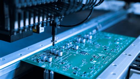
In the realm of PCB assembly, integrating data analytics has become a cornerstone for achieving high-yield production and minimizing defects. By systematically collecting and analyzing data from SMD assembly workflows, manufacturers can identify patterns, predict potential bottlenecks, and refine processes in real time. For instance, sensors embedded in PCBA lines capture metrics such as solder paste deposition accuracy, component placement alignment, and reflow oven temperature profiles. These datasets enable teams to pinpoint deviations from optimal parameters, allowing for immediate corrective actions. Advanced machine learning algorithms further enhance this capability by correlating historical performance data with quality outcomes, enabling predictive maintenance and reducing unplanned downtime.
The application of statistical process control (SPC) tools ensures that variations in SMD assembly remain within acceptable tolerances, while root-cause analysis helps address recurring defects. Real-time dashboards provide visibility into key performance indicators (KPIs), such as first-pass yield and defects per million opportunities (DPMO), empowering decision-makers to prioritize improvements. Additionally, integrating data analytics with automated inspection systems creates a closed-loop feedback mechanism, where inspection results directly inform process adjustments. This synergy between data-driven insights and PCBA workflows not only enhances precision but also reduces material waste and operational costs.
By fostering a culture of continuous improvement, manufacturers can iteratively optimize PCB assembly lines, ensuring scalability and adaptability to evolving design requirements. The result is a streamlined production ecosystem where efficiency and quality coexist, driving long-term competitiveness in the electronics manufacturing landscape.
Case Studies: Successful High-Yield SMD Assembly Implementations
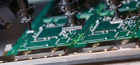
Several leading manufacturers have demonstrated how optimized PCB SMD assembly workflows can significantly boost production yield while minimizing defects. For instance, a prominent automotive electronics supplier faced recurring issues with component misalignment during PCBA processes. By integrating vision-guided placement systems and high-precision solder paste dispensers, they achieved a 98.5% placement accuracy rate, reducing rework costs by 40%. This approach highlights the critical role of automated inspection systems, such as 3D AOI (Automated Optical Inspection), in identifying micro-scale soldering defects before final testing.
Another case involved a consumer electronics firm struggling with inconsistent throughput in high-mix, low-volume production. By redesigning their PCB assembly workflow layout to minimize material handling delays and adopting modular conveyor systems, they cut cycle times by 25%. Additionally, leveraging data analytics to monitor solder joint quality in real-time allowed them to adjust reflow oven profiles dynamically, slashing thermal-related defects by 60%.
In the aerospace sector, a manufacturer tackled challenges with miniaturized components by implementing laser-cut stencils and nitrogen-assisted reflow soldering. This not only improved solder joint reliability but also enabled tighter tolerances for 0201 metric components, critical for space-constrained applications. Post-implementation, their first-pass yield surged from 82% to 94%, with a 30% reduction in material waste.
These examples underscore the importance of holistic process integration—combining advanced machinery, intelligent inspection, and data-driven adjustments—to optimize SMD assembly outcomes. By prioritizing material traceability and vendor collaboration, these manufacturers also mitigated supply chain risks, ensuring consistent quality across high-volume PCBA runs. Such strategies prove that precision, automation, and continuous improvement are indispensable for achieving high-yield production in modern electronics manufacturing.
Conclusion
In the rapidly evolving landscape of modern electronics, PCB assembly and PCBA processes play a pivotal role in delivering reliable, high-performance devices. Streamlining SMD assembly workflows requires a holistic approach that integrates precision, automation, and data-driven decision-making. By adopting advanced techniques such as automated optical inspection (AOI) and high-speed pick-and-place systems, manufacturers can achieve exceptional accuracy in component placement and soldering, directly contributing to higher production yields. Equally critical is the optimization of workflow layouts, which minimizes bottlenecks and enhances throughput while maintaining rigorous quality standards. Material selection, particularly for solder paste and substrates, further ensures cost-efficiency without compromising durability or performance. Leveraging data analytics to monitor real-time process metrics enables continuous refinement, identifying trends that preempt defects and reduce rework. Case studies across industries demonstrate that integrating these strategies not only slashes operational costs but also fortifies supply chain resilience. As demand for compact, high-density electronics grows, the ability to balance speed, precision, and scalability in SMD assembly will remain a cornerstone of competitive manufacturing. The future of PCB assembly lies in embracing innovation while fostering collaboration across design, engineering, and production teams to meet the ever-increasing expectations for quality and efficiency.
Frequently Asked Questions
What are the primary challenges in modern PCB assembly processes?
The main challenges include achieving high-precision component placement, minimizing soldering defects, managing thermal profiles, and ensuring consistent material quality. SMD components demand tight tolerances, and even minor misalignments can lead to failures in PCBA boards.
How can automated inspection systems improve PCB SMD assembly yield?
Automated optical inspection (AOI) and X-ray inspection systems detect defects like solder bridging, missing components, or misaligned parts early in the process. This reduces rework costs and ensures compliance with high-reliability standards for PCBA products.
What role does workflow optimization play in reducing operational costs?
Efficient workflow design minimizes bottlenecks, reduces component handling, and accelerates throughput. For example, arranging pick-and-place machines and reflow ovens in a linear sequence cuts idle time, enhancing overall production efficiency in PCB assembly lines.
How does material selection impact SMD assembly quality?
Using high-quality solder paste, adhesives, and substrates ensures reliable electrical connections and thermal stability. Poor materials can cause delamination or voiding, leading to failures in PCBA units under stress.
Can data analytics really improve PCB SMD assembly outcomes?
Yes. Real-time monitoring of placement accuracy, solder paste volume, and reflow temperatures allows for rapid adjustments. Predictive analytics also identifies trends, enabling proactive maintenance and reducing downtime in PCBA production.
What are the benefits of modular PCB assembly setups?
Modular designs allow quick reconfiguration for different product batches, supporting flexible manufacturing. This is critical for industries requiring rapid prototyping or mixed-volume PCBA orders.
Ready to Elevate Your PCB SMD Assembly Workflow?
Explore tailored solutions for high-yield production and defect reduction. Click here to discover how advanced PCBA strategies can transform your manufacturing process.
