PCB (Printed Circuit Board) Overview
Introduction
Printed Circuit Board (PCB) is an indispensable component of modern electronic devices. It not only provides mechanical support for electronic components, but also realizes electrical connection through conductive lines. With the continuous development of science and technology, the design and manufacturing technology of PCB is also constantly improving, driving electronic products to develop in the direction of smaller size, higher performance and more multifunctionality.
Basic structure of PCB
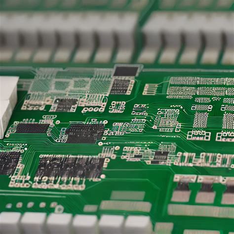
PCB is usually composed of insulating substrate and conductive lines. The insulating substrate generally uses FR-4 (glass fiber reinforced epoxy resin) material, while the conductive line is usually a copper layer. The basic structure of PCB can be divided into the following parts:
Substrate: The substrate is the foundation of PCB and provides mechanical support. Common substrates include FR-4, CEM-1, CEM-3, etc.
Conductive layer: The conductive layer is the core part of PCB and is responsible for the transmission of electrical signals. The copper layer can be formed by processes such as electroplating and etching.
Insulating layer: The insulating layer is used to isolate different conductive lines to prevent short circuits and signal interference.
Surface treatment: In order to improve solderability and prevent oxidation, the surface of the PCB is usually treated, such as HASL (hot air leveling), ENIG (electroless nickel gold plating), etc.
Types of PCBs
PCBs can be divided into many types according to different application requirements:
Single-sided board: Only one side has conductive lines, suitable for simple electronic products, such as small household appliances.
Double-sided board: Both sides have conductive lines, connected by holes, suitable for medium-complexity circuits.
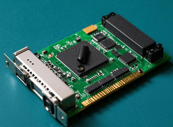
Multilayer board: It consists of three or more layers of conductive layers and insulating layers, suitable for high-density, high-performance electronic products, such as computer motherboards and communication equipment.
Flexible PCB: Made of flexible materials, it can be bent and folded, suitable for applications with limited space, such as smartphones and wearable devices.
Rigid-flexible board: It combines the advantages of rigid and flexible PCBs and is suitable for complex electronic systems.
PCB design process
PCB design is a complex process, which usually includes the following steps:
Schematic design: Use electronic design automation (EDA) tools to draw the schematic diagram of the circuit and determine the connection relationship of each component.
PCB layout: According to the schematic diagram, electronic components are placed on the PCB and laid out reasonably to reduce signal interference and improve heat dissipation.
PCB routing: According to the layout, the conductive lines are connected to form a complete circuit. This process needs to consider issues such as signal integrity and power distribution.
Design verification: Use simulation tools to verify the design to ensure that the function and performance of the circuit meet the requirements.
Generate production files: Convert the design to the file format required for production, such as Gerber files, to facilitate production by PCB manufacturers.
PCB manufacturing process
The manufacturing process of PCB mainly includes the following steps:
Material preparation: Select suitable substrates and copper foils to prepare the materials required for production.
Graphic transfer: Use photolithography technology to transfer the design graphics to the substrate to form a pattern of conductive lines.
Etching: Remove the excess copper layer through chemical etching, leaving only the required conductive lines.
Electroplating: A layer of copper is plated in the holes and on the lines to increase conductivity and mechanical strength.
Surface treatment: Treat the surface of the PCB to improve solderability and prevent oxidation.
Cutting and testing: Cut the PCB into the required size and conduct electrical testing to ensure that it functions properly.
Application areas of PCB
PCB is widely used in various fields, including but not limited to:
Consumer electronics: such as mobile phones, tablets, TVs, etc.
Computers: motherboards, graphics cards, hard drives, etc.
Communication equipment: routers, switches, base stations, etc.
Automotive electronics: car navigation, entertainment systems, engine control units, etc.
Medical equipment: monitors, diagnostic equipment, medical imaging equipment, etc.
Future development trends of PCB
With the continuous advancement of science and technology, the PCB industry is also developing continuously, and the main trends include:
High frequency and high speed: With the development of 5G and the Internet of Things, the demand for high-frequency and high-speed PCBs is increasing, and the design and manufacturing processes are also constantly improving.
Miniaturization: As electronic products develop towards miniaturization, the size and thickness of PCBs are also gradually decreasing.
Environmentally friendly materials: With the improvement of environmental awareness, PCB manufacturers have begun to use environmentally friendly materials to reduce the impact on the environment.
Intelligence: Intelligent PCBs (such as embedded sensors) will become the future development direction, promoting the development of smart homes and industrial automation.
Conclusion
Printed circuit boards (PCBs) are core components of modern electronic devices, and the advancement of their design and manufacturing technology directly affects the performance and functions of electronic products. With the continuous development of science and technology, PCBs will play an important role in a wider range of fields. Understanding the basic knowledge and development trends of PCBs is of great significance for professionals and enthusiasts in the electronics industry.