High-speed PCB design – layout
Looking at successful electronic products, they basically have five characteristics:
1. Stable performance;
2. Overall beauty;
3. Easy to use;
4. Reasonable cost;
5. Convenient mass production;
If you focus on any one of these points, it cannot be called a successful product. These five points are all related to the layout. In other words, a good and reasonable layout is to fully consider the above five points, so the layout is a very important part of the success of the product.
In high-speed PCB design, layout is even more important.
Its rationality is directly related to subsequent wiring, signal transmission quality, EMI, EMC, ESD and other issues, which are related to the success or failure of product design. The specific steps can be done according to the initial layout first and then the detailed layout.
The work to be done in the initial layout is mainly to divide the principle into reasonable areas on the PCB board according to the function.
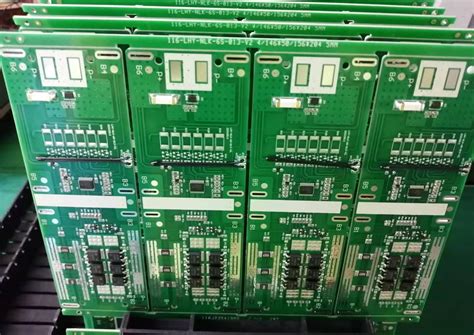
First, place the main components in the corresponding area
. During the placement process, the heat dissipation problem should be considered. There should be gaps between the components.
If there is a fan, pay attention to the direction of the air outlet, and let the wind blow to the components with high heat generation and a larger range as much as possible; the weight of the entire PCB board should be balanced to avoid the distortion of the PCB board after the components are installed, which will bring great hidden dangers to the product quality; for those with structural restrictions, pay attention to the placement of components with fixed positions, and meet the requirements of height-restricted areas and prohibited areas.
The detailed layout can be done according to the following points,
First, after the initial layout, the remaining components should be placed in the area divided during the initial layout according to the function of each part of the circuit. The position of the components cannot be determined simply by the mouse line between the components on the PCB board. Reasonable placement of bypass capacitors, decoupling capacitors, energy storage capacitors, impedance matching resistors, anti-ESD components and other components should allow these components to fully play their application role.
Second, directional components can only have two directions at most, and non-directional components should be aligned in the center when in a row, which is convenient for production and beautiful.
Third, for components with a certain height, in addition to considering the height limit area, it is also necessary to consider that it should not affect the plugging and unplugging of other connectors and the use with other peripherals.
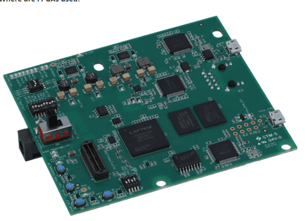
the components should be placed with a certain gap, and the distance from the edge of the board should be kept at 120mil (this spacing can be adjusted according to the process level of the processing plant; if the PCB itself has an additional process edge, this spacing can be ignored). For PCBs with SMD components on the back, the SMD components should be kept at a distance of 80mil from the DIP component feet (this spacing can be adjusted according to the process level of the processing plant) to facilitate debugging, production and heat dissipation.
Fifth, for highly sensitive circuits and components
a certain distance should be maintained from other circuits to avoid mutual interference, such as clock chips and related components, crystals, switching power supplies, inductors, etc.; there should also be enough space between components with high heat generation to facilitate air circulation and a large area of copper foil can be laid behind to dissipate heat.
Sixth, analog circuits and digital circuits should be placed in separate areas and keep a certain distance to avoid mutual interference
the I/O related circuits should be placed as close to the edge of the PCB as possible, which is conducive to the interference leaving the internal circuit of the PCB as soon as possible. Filtering and anti-ESD devices should be placed around the I/O circuits to filter out interference entering from the interface and protect the circuits in the PCB from damage by electrostatic discharge.

