pcba assy

Key Takeaways
The PCBA ASSY process integrates PCB assembly with component placement and soldering to create functional electronic circuits. Key considerations include selecting high-quality materials, adhering to design specifications, and implementing rigorous quality control protocols. Below are essential insights:
- PCBA (Printed Circuit Board Assembly) involves mounting components like resistors, capacitors, and ICs onto a PCB (Printed Circuit Board) using techniques such as surface-mount technology (SMT) or through-hole assembly.
- A streamlined PCBA workflow typically includes solder paste application, component placement, reflow soldering, and post-assembly testing.
- Testing methods like automated optical inspection (AOI) and in-circuit testing (ICT) are critical for identifying defects early.
| Factor | PCBA | PCB |
|---|---|---|
| Function | Fully assembled with components | Bare board without components |
| Complexity | Higher due to component integration | Lower, focusing on layout design |
| Testing Focus | Functional performance | Electrical connectivity |
Tip: Always validate design files (e.g., Gerber, BOM) before initiating PCBA manufacturing to avoid costly rework.
Emerging trends such as miniaturization and IoT integration are driving advancements in PCBA technology, emphasizing the need for precision and scalability. Understanding the distinction between PCBA and PCB ensures clarity in project planning, as the former represents the final functional product, while the latter is its foundational substrate.
Introduction to PCBA Assembly Process
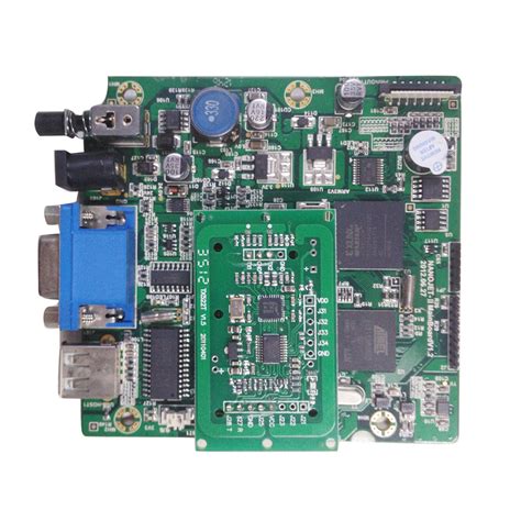
The PCBA (Printed Circuit Board Assembly) process is a critical phase in electronics manufacturing, transforming bare PCB (Printed Circuit Board) substrates into functional electronic systems. This process involves mounting and soldering electronic components—such as resistors, capacitors, integrated circuits, and connectors—onto the board to create a fully operational assembly. Modern PCB assembly techniques rely heavily on automated machinery, including surface-mount technology (SMT) equipment for high-speed placement of miniature components and reflow ovens for precise soldering. The workflow typically begins with solder paste application, followed by component placement, soldering, and rigorous quality control checks to ensure reliability.
A key distinction between PCBA and standalone PCB lies in the integration of active and passive components. While a PCB serves as the foundational platform with conductive pathways, a PCBA represents the completed, functional unit ready for integration into end products. Design considerations, such as thermal management, signal integrity, and component spacing, play a vital role in optimizing the assembly process. Advanced testing methods, including automated optical inspection (AOI) and functional testing, are employed to detect defects and validate performance. As industries demand smaller, faster, and more complex devices, innovations in PCBA technology—such as 3D printing of circuits and flexible PCB assemblies—continue to push the boundaries of modern electronics manufacturing.
Key Components in PCBA ASSY Manufacturing
The PCBA (Printed Circuit Board Assembly) manufacturing process relies on several critical components to ensure functionality and reliability. At its core, the printed circuit board (PCB) serves as the foundation, providing mechanical support and electrical connectivity through conductive pathways. Key electronic components, such as resistors, capacitors, integrated circuits (ICs), and connectors, are mounted onto the PCB during the PCB assembly process. Surface-mount devices (SMDs) and through-hole components are two primary types used, with SMDs dominating modern designs due to their compact size and compatibility with automated assembly.
Soldering materials, including solder paste and flux, play a vital role in creating durable electrical connections. Advanced PCBA workflows often incorporate pick-and-place machines for precise component positioning and reflow ovens for controlled soldering. Additionally, ball grid arrays (BGAs) and quad flat packages (QFPs) are frequently employed for high-density interconnects, demanding meticulous alignment during assembly.
Supporting elements like test points, fiducial markers, and thermal management materials (e.g., heat sinks or thermal pads) ensure quality and longevity. The integration of programmable logic devices (PLDs) and microcontrollers further enhances the board’s adaptability in complex applications. For industries requiring ruggedized electronics, conformal coatings protect the assembly from environmental stressors like moisture or dust.
Efficient PCB assembly also depends on design-specific parts, such as connectors for external interfaces or power regulators for voltage stabilization. Each component must adhere to strict tolerances to avoid defects, underscoring the importance of material selection and process control in PCBA manufacturing. By harmonizing these elements, manufacturers achieve assemblies that meet both performance benchmarks and industry standards.
Steps Involved in PCBA Assembly Workflow
The PCBA assembly workflow encompasses a sequence of meticulously coordinated steps designed to convert a bare PCB into a fully operational electronic module. The process begins with solder paste application, where a stainless-steel stencil deposits a precise layer of solder paste onto the board’s contact pads. This step is crucial for establishing reliable electrical connections during subsequent stages. Following this, pick-and-place machines automate the placement of surface-mount devices (SMDs) and through-hole components onto the PCB. These machines ensure high-speed, accurate positioning, which is vital for maintaining consistency in high-volume production. The assembled board then enters a reflow oven, where controlled thermal profiles melt the solder paste, forming permanent bonds between components and the PCB.
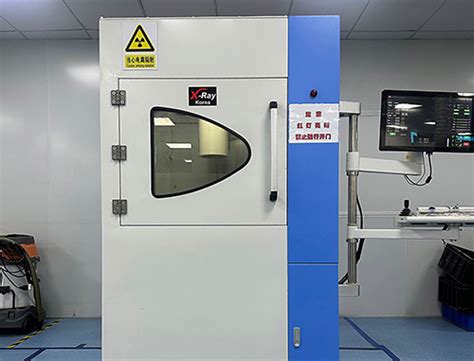
After soldering, the assembly undergoes rigorous inspection. Automated optical inspection (AOI) systems use advanced cameras to detect placement errors, solder bridging, or missing components, while X-ray inspection examines hidden joints, such as those beneath ball grid array (BGA) packages. Functional testing follows, where the PCBA is powered and subjected to simulated operational conditions to validate performance metrics like voltage, current, and signal integrity. Depending on the application, additional steps such as conformal coating may be applied to protect the assembly from moisture, dust, or thermal stress. Each phase in the PCB assembly process is interdependent, emphasizing the need for precision and quality control to ensure the final PCBA meets industry standards and end-user requirements.

Quality Control and Testing for PCBA ASSY
Ensuring reliability and performance in PCB assembly requires rigorous quality control and testing protocols. Modern PCBA manufacturing integrates automated inspection techniques such as Automated Optical Inspection (AOI) and X-ray Inspection (AXI) to detect solder joint defects, component misalignment, or bridging. These systems analyze PCB layouts against design specifications, flagging discrepancies early in the production cycle. Functional testing follows, where assembled boards undergo simulated operational conditions to verify electrical performance, signal integrity, and power distribution. For high-reliability applications, environmental stress screening (ESS)—including thermal cycling and vibration tests—ensures durability under extreme temperatures or mechanical shocks.
Statistical process control (SPC) methods track manufacturing metrics, such as solder paste deposition accuracy and component placement precision, to maintain consistency across batches. Additionally, adherence to industry standards like IPC-A-610 and ISO 9001 guarantees compliance with global quality benchmarks. Advanced PCBA providers also employ boundary-scan testing to diagnose complex integrated circuits, reducing fault isolation time. By combining automated tools with manual audits, manufacturers minimize defects, optimize yield, and deliver PCB assemblies that meet stringent functional and longevity requirements.
Design Considerations for Optimal PCBA Assembly
Effective PCBA design is critical to ensuring both functionality and manufacturability in electronics production. A well-planned layout begins with optimizing component placement to minimize signal interference and thermal hotspots, which directly impacts reliability and performance. Designers must prioritize PCB assembly-friendly practices, such as adhering to standardized footprints and maintaining adequate spacing between components to avoid soldering defects. Additionally, selecting materials with appropriate thermal and electrical properties is essential, especially for high-frequency or high-power applications.
Routing considerations play a pivotal role in PCBA success. Proper trace width, impedance matching, and via placement help mitigate electromagnetic interference (EMI) and ensure signal integrity. Integrating Design for Manufacturability (DFM) principles early in the process reduces risks like mismatched pad sizes or insufficient clearance, which can lead to costly rework. Collaboration between design and manufacturing teams is vital to address potential bottlenecks, such as complex solder mask requirements or challenges in automated component placement.
Another critical aspect is thermal management. Designers must incorporate heat dissipation strategies, such as thermal vias, heatsinks, or copper pours, to prevent overheating in densely packed PCB assemblies. Testing prototypes under real-world conditions helps validate thermal and electrical performance before full-scale production. Finally, documentation clarity—including detailed assembly drawings and bill of materials (BOM)—ensures seamless translation from design to PCBA execution, reducing errors and accelerating time-to-market.

Applications of PCBA ASSY in Modern Electronics
The PCBA ASSY (Printed Circuit Board Assembly) process plays a pivotal role in powering the devices that define today’s technological landscape. From consumer electronics to industrial machinery, PCB assembly enables the integration of complex circuits into compact, functional units. In smartphones, for instance, PCBA units manage everything from signal processing to power distribution, ensuring seamless connectivity and performance. Similarly, automotive systems rely on advanced PCB assembly techniques to support features like advanced driver-assistance systems (ADAS), infotainment, and electric vehicle battery management. The precision and reliability of PCBA are critical here, as these systems operate under extreme temperatures and vibrations.
Medical devices further highlight the versatility of PCBA ASSY, where high-density interconnects and miniaturized components enable life-saving equipment such as pacemakers, imaging systems, and portable diagnostics. Industrial automation also benefits from robust PCB assembly solutions, with programmable logic controllers (PLCs) and sensors depending on durable, high-performance assemblies to maintain operational efficiency. Additionally, the rise of IoT (Internet of Things) devices underscores the importance of PCBA in creating interconnected smart systems, from home automation to environmental monitoring.
In aerospace and defense, PCBA assemblies must meet stringent standards for durability and accuracy, as they are deployed in satellites, avionics, and communication systems. The adaptability of PCB assembly processes—whether through surface-mount technology (SMT) or through-hole methods—ensures compatibility with diverse design requirements. As industries continue to prioritize miniaturization and energy efficiency, the role of PCBA ASSY in enabling innovative electronics remains indispensable, bridging the gap between theoretical design and real-world functionality.

PCBA vs. PCB: Understanding the Differences
While the terms PCB (Printed Circuit Board) and PCBA (Printed Circuit Board Assembly) are often used interchangeably, they represent distinct stages in electronics manufacturing. A PCB is the foundational, non-populated board composed of insulating substrates and conductive copper traces that form electrical pathways. In contrast, PCBA refers to the completed assembly where components such as resistors, capacitors, integrated circuits, and connectors are mounted and soldered onto the PCB, transforming it into a functional electronic circuit.
The primary difference lies in their roles: a PCB serves as the structural and electrical backbone, while PCBA represents the operational system ready for integration into devices. The PCB assembly process involves multiple stages, including solder paste application, component placement via Surface Mount Technology (SMT) or through-hole insertion, reflow soldering, and rigorous testing. These steps ensure the PCBA meets performance specifications and reliability standards.
Design considerations also vary between the two. PCB design focuses on trace routing, layer stack-up, and thermal management, whereas PCBA design emphasizes component placement, solder joint integrity, and compatibility with automated assembly equipment. For instance, component spacing and footprint accuracy become critical in PCBA to avoid manufacturing defects.
In applications, standalone PCBs are rare outside prototyping, as most electronics require populated boards. PCBA is integral to devices ranging from consumer gadgets to industrial machinery, where functionality depends on the seamless interaction of components. Understanding this distinction is vital for optimizing manufacturing workflows, cost estimation, and troubleshooting in electronics production.
Emerging Trends in PCBA Assembly Technology
The landscape of PCBA (Printed Circuit Board Assembly) technology is rapidly evolving, driven by advancements in automation, materials science, and demand for higher-performance electronics. One notable trend is the integration of miniaturized components, enabling compact designs without compromising functionality. This shift is supported by innovations in surface-mount technology (SMT), which allows precise placement of smaller components like microcontrollers and high-density interconnects (HDIs). Additionally, the adoption of AI-driven inspection systems has revolutionized quality control, reducing defects in PCB assembly workflows by identifying microscopic flaws in real time.
Another emerging development is the use of flexible and rigid-flex PCBA solutions, catering to wearable devices and IoT applications. These designs require specialized PCB assembly techniques to ensure durability under bending or dynamic conditions. Environmentally conscious practices are also gaining traction, with manufacturers prioritizing lead-free soldering and recyclable materials to meet global sustainability standards.
The rise of Industry 4.0 has further transformed PCBA processes through smart factories equipped with IoT-enabled machinery. These systems enable predictive maintenance, minimizing downtime and optimizing production efficiency. Furthermore, advancements in thermal management materials, such as high-conductivity substrates, address heat dissipation challenges in high-power applications like electric vehicles and 5G infrastructure.
Collaboration between PCB assembly providers and designers is increasingly critical, as design-for-manufacturability (DFM) principles ensure seamless translation of schematics into functional assemblies. As the demand for faster, smaller, and more reliable electronics grows, the PCBA industry continues to innovate, blending cutting-edge technologies with sustainable practices to shape the future of electronics manufacturing.
Conclusion
The PCBA ASSY process represents a critical phase in modern electronics manufacturing, bridging the gap between design and functional end products. As the backbone of devices ranging from consumer gadgets to industrial systems, PCB assembly requires meticulous attention to detail across design, component placement, soldering, and testing. The integration of advanced technologies such as automated pick-and-place systems and reflow soldering has streamlined production, enabling high precision and scalability. However, success in PCBA hinges on robust quality control measures, including automated optical inspection (AOI) and functional testing, to ensure reliability and compliance with industry standards.
Design considerations like thermal management, component spacing, and material selection play pivotal roles in optimizing PCBA outcomes, while emerging trends such as miniaturization and IoT-driven smart manufacturing continue to reshape the landscape. Distinguishing PCBA from bare PCB is essential—while a PCB serves as the physical platform, PCBA encompasses the entire process of populating and testing the board, transforming it into a functional unit. As industries demand faster turnaround times and higher complexity, innovations in flexible PCB assembly and sustainable manufacturing practices are poised to address these challenges, ensuring PCBA remains at the forefront of technological advancement.
Frequently Asked Questions
What is the difference between a PCB and a PCBA?
A PCB (printed circuit board) is a bare board with conductive pathways but no components. A PCBA (printed circuit board assembly) refers to the completed board after components like resistors, capacitors, and ICs are soldered onto the PCB through the pcb assembly process.
What are the key steps in the PCBA workflow?
The pcb assembly process typically includes solder paste application, component placement via surface-mount technology (SMT) or through-hole technology (THT), reflow soldering, inspection, and functional testing. Automated machinery ensures precision in high-volume production.
How is quality ensured during PCBA manufacturing?
Quality control involves automated optical inspection (AOI), X-ray inspection for hidden flaws, and electrical testing to verify performance. Strict adherence to IPC standards guarantees reliability and functionality of the final PCBA.
What design factors optimize PCBA assembly?
Designers should prioritize component spacing, thermal management, and clear silkscreen markings. Using design for manufacturability (DFM) principles minimizes errors and reduces costs during the pcb assembly phase.
Where are PCBA assemblies commonly used?
PCBA is integral to modern electronics, including smartphones, medical devices, automotive systems, and IoT gadgets. Its versatility supports both low-volume prototyping and mass production.
What trends are shaping PCBA technology?
Advancements include miniaturization of components, adoption of flexible PCBs, and AI-driven inspection tools. Eco-friendly practices, such as lead-free soldering, are also gaining prominence in pcb assembly workflows.
Explore Professional PCBA Assembly Solutions Today!
For tailored pcb assembly services that prioritize quality and efficiency, please click here to connect with experts who can bring your electronic designs to life.