Why is it so difficult to design RF and microwave PCBs? You should master these tips
Introduction
Today’s electronic products are no longer like the TVs and refrigerators of the 1970s, which consumers only replaced every ten years. Now almost every member of every family is a consumer of electronic products, and as technological development continues to bring a variety of affordable new features to smartphones, tablets, cars and TVs, people buy new products every year.
One of the common characteristics of these electronic products is the use of wireless technology, which is extremely dependent on RF radio frequency circuits. Unfortunately, even the most confident designers are often daunted by RF circuits because it brings huge design challenges and requires professional design and analysis tools. Because of this, for many years, the RF part of the PCB has been designed by independent designers with RF design expertise.
Why is it so difficult to design RF and microwave PCBs?
The problems that arise in this design process are numerous and can have a serious impact on quality and productivity. For example, when embedding one designer’s RF circuit into another designer’s PCB, efficiency is bound to be greatly reduced because they often use different design formats. Designers are also often forced to make changes in their designs to accommodate RF circuits. Because simulations are often performed within the context of the RF circuit, rather than the entire PCB, significant impacts of the board on the RF circuit, and vice versa, can be missed.
As RF content continues to increase, PCB designers and engineers realize that to improve productivity and product quality, RF design challenges are best solved within their own design tools. Unfortunately, most desktop PCB design tools do not make this task easy for them.
For example, after a circuit is modeled using an RF simulator, once the desired electrical performance is achieved, the simulator generates copper shapes for this circuit (usually in DXF format) for import into the PCB design tool. This process often causes some confusion for designers, such as not being able to convert the DXF file to copper shapes due to the inability to convert it correctly. In this case, the designer needs to manually import the DXF file, which may cause human errors and errors in shape size, resulting in failure of the RF circuit.
The challenges faced by PCB designers or engineers when trying to layout RF and microwave circuits are far more than just the above. Fortunately, there are some small solutions in your design tools that can play an important role in resolving the above challenges. This white paper will introduce you to six tips to help you simplify any RF PCB design task and reduce the pressure of work!
- Maintain good, accurate RF shapes
Serious errors such as those described above can cause poor circuit performance or even non-functioning. To minimize errors, simplify RF design tasks, and increase productivity, PCB design tools can provide import control for complex copper shapes. For example, you can create usable copper shapes by controlling the layers in the DXF file and re-mapping them to the CAD electrical system layers (Figure 1).
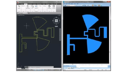
Figure 1: Design tools that allow users to control the DXF import process will help reduce human errors and errors, such as when the imported file cannot be converted to copper shapes due to excessive complexity.
- Keep corners sharp
An important aspect of designing copper shapes for RF and microwave is the ability to create Gerber files with sharp corners. Good PCB design tools can simplify this process. For example, using 50mm lines to draw a shape will often result in a design with a smaller radius than using a 50mm circular aperture. Design tools can achieve sharp corners by automatically converting line widths correctly when creating Gerber files (Figure 2).
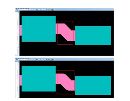
Figure 2: Effective PCB design tools automatically consider the line type used to draw the shape to calculate the correct line width, making it easy for you to create sharp corners.
- Automatically Generate Chamfered Corners
Chamfers are often used in RF and microwave circuits to reduce the impedance of the segmented discontinuity between the supply line and the capacitor, thereby improving the frequency performance of the MMIC. The distance between the 90º corner and the chamfer is critical. Therefore, designers need an automatic method to specify the required chamfer ratio based on the design. Designers and engineers will benefit from the ability of PCB design tools to automatically enforce the required chamfer ratio based on design rules, saving time and improving design quality (Figure 3).
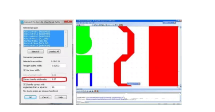
Figure 3: The ability to set chamfer rules can simplify the design process and save time.
- USE AUTOMATION TO HELP LAY OUT COPLANAR AND CHANNEL WAVEGUIDES
Coplanar and channel waveguides are also common in RF and microwave design. This task can be very time-consuming and error-prone when created manually. Designers need to control the specific distance between traces and vias, as well as the distance between one via and another, to ensure that the circuit has the performance required by the design. Design tools can also help in this regard, that is, by providing via usage control and automating the use of vias to reduce complexity and improve quality (Figure 4).
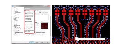
Figure 4: If PCB design tools can control the creation of coplanar and wave-guide vias, it will help significantly reduce design errors and shorten design time.
- USE AUTOMATIC STITCHING VIAS
Another important aspect of RF design is to ensure that vias are properly used to shield specific areas. Although this task can be performed manually by designers, it is an extremely time-consuming process. If PCB design tools can complete this process automatically, it will shorten the design cycle time and ensure that all your design rules are met. With such tools, designers can specify specific rules for via pattern generation and let the PCB design tool do the rest.
- Use design rules to ensure “correct by design”
PCB design tools that support RF design typically allow for multiple design rules to be set: the type of vias used for different copper areas; the type of nets to which the vias themselves need to connect; the distance from the edge of the copper area to the vias that needs to be maintained; the distance from one via to the next; the type of via pattern; and whether a Faraday cage can be generated by simply adding vias to the outer edge of the copper area (Figure 5).
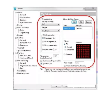
Figure 5: With PCB design tools that support RF design, you can set design rules for via pattern generation and automatically enforce them in your design, saving you time and ensuring that all your design rules are met.
Conclusion
Today’s designers and engineers face increasing design challenges, so it is necessary to have a PCB design tool that can efficiently support RF and microwave design. Manually creating complex copper shapes, chamfers, and via patterns is a time-consuming and error-prone process. By improving the ability to manipulate RF and microwave elements using effective design tools, designers can focus on implementing more functionality and reducing device size while maintaining high product quality.