Optimizing SMT Board Assembly for Modern Electronics Manufacturing
Key Takeaways
Modern PCB assembly processes demand meticulous attention to detail across multiple technical domains. For PCBA manufacturing success, engineers must balance precision, thermal dynamics, and quality control while leveraging emerging technologies. Below are critical considerations for optimizing surface-mount technology workflows:
"Effective SMT optimization begins with understanding the interplay between design choices and production realities. Always prioritize design for manufacturability principles early in the development cycle."
– Industry Process Engineer
Foundational Optimization Strategies
Component Placement Precision
High-density layouts require sub-micron placement accuracy using vision-aligned pick-and-place systems. Implement 3D solder paste inspection to verify deposition quality before component mounting.Thermal Management Integration Strategy Implementation Yield Impact Thermal relief patterning 45° spoke designs in ground planes +12% Active cooling alignment Component orientation relative to airflow +8% Automated Quality Assurance
Modern AOI systems (Automated Optical Inspection) reduce human error by 63% in PCBA verification processes. Combine with X-ray inspection for hidden joint analysis in BGA packages.
Process Enhancement Tactics
- Solder paste optimization: Maintain viscosity between 800–1,200 kcps for consistent stencil release
- Stencil design rules:
- Aspect ratio >1.5 for reliable aperture release
- Area ratio >0.66 for micro-BGA applications
Pro Tip: Conduct tribological analysis of solder paste behavior under different environmental conditions to refine stencil specifications.
Emerging machine learning applications now predict solder joint reliability with 94% accuracy by analyzing historical process data. This enables predictive maintenance of placement equipment and real-time thermal profile adjustments in reflow ovens.
When troubleshooting common defects like tombstoning or voiding, adopt a systemic approach:
- Verify solder paste printing registration (±25µm tolerance)
- Profile reflow zones against component thermal limits
- Audit moisture-sensitive device handling protocols
These interconnected strategies underscore the importance of viewing PCB assembly as a holistic system rather than isolated process steps. By integrating advanced process controls with robust DFM practices, manufacturers can achieve first-pass yields exceeding 99.2% in high-mix production environments.
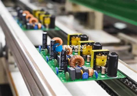
Precision Component Placement Techniques for High-Density SMT Assembly
Achieving optimal results in PCB assembly demands meticulous attention to component placement, particularly in high-density PCBA designs where millimeter-scale accuracy determines functionality and reliability. Modern surface-mount technology (SMT) lines leverage vision-aligned pick-and-place systems with ±25µm repeatability, enabling the precise positioning of micro-BGA packages, 0201 passives, and QFN components. These systems integrate real-time laser profilometry to verify coplanarity, critical for avoiding tombstoning defects in ultra-fine-pitch applications.
A key advancement lies in dynamic feeder synchronization, which minimizes nozzle travel time during PCB assembly by optimizing component retrieval sequences. For mixed-technology boards containing both 0.4mm-pitch CSPs and through-hole connectors, dual-lane placement architectures maintain throughput above 30,000 components per hour without compromising placement accuracy. Thermal management begins at this stage, with pick-and-place machines employing heated nozzles (maintained at 35-45°C) to prevent adhesive curing delays in moisture-sensitive devices.
The rise of PCBA designs with embedded actives necessitates 3D laser mapping for pre-placement board warpage detection. Systems like Fuji NXT III and ASM SIPLACE TX utilize this data to dynamically adjust Z-axis placement pressure, ensuring consistent solder paste collapse patterns across uneven substrates. For 01005 components and smaller, vacuum-assisted placement heads with <5ms response times prevent positional drift caused by air turbulence during high-speed operations.
Machine learning-enhanced collision avoidance algorithms now process real-time telemetry from 12-axis robotic arms, enabling safe operation at 1.2g acceleration rates even in complex multi-nozzle configurations. This capability proves vital when assembling hybrid rigid-flex PCB assemblies, where board flexure requires continuous trajectory recalibration. Post-placement verification employs high-magnification coaxial illumination to detect sub-50µm misalignments before reflow, reducing downstream rework costs by up to 18% in automotive-grade applications.
As component densities increase, multi-stage fiducial recognition systems compensate for local positional deviations caused by CTE mismatches in multilayer boards. Advanced PCBA workflows integrate this placement data with downstream processes, creating closed-loop feedback for solder paste volume adjustments—a critical link to subsequent thermal management and inspection phases in the SMT value chain.
Thermal Management Solutions in SMT Board Assembly Processes
Effective thermal management has become a critical focus in SMT board assembly as modern electronics demand higher power densities and miniaturization. The interplay between component placement, material selection, and heat dissipation directly impacts the reliability of PCBA outcomes. With devices shrinking and power requirements escalating, engineers must balance thermal conductivity and mechanical stability to prevent failures such as solder joint degradation or component delamination.
A primary strategy involves optimizing PCB assembly layouts to incorporate thermally conductive substrates like metal-core or ceramic-filled laminates. These materials enhance heat transfer away from high-power components such as FPGAs or power regulators. Advanced thermal interface materials (TIMs)—including graphene-enhanced pads or phase-change compounds—are now widely adopted to bridge gaps between heat-generating components and heatsinks, improving thermal pathways by up to 40% compared to traditional greases.
Reflow soldering processes also require precise thermal profiling to avoid uneven heat distribution. Modern SMT assembly lines employ dynamic zone-controlled ovens that adjust temperatures in real time, accounting for variations in component mass and board topography. This ensures consistent solder joint formation while mitigating thermal shock risks. Post-assembly, infrared thermography and AI-driven thermal simulation tools analyze heat maps to identify hotspots, enabling iterative design improvements.
For high-reliability applications, active cooling solutions such as micro-fans or vapor chambers are integrated during PCBA design phases. These systems work synergistically with passive methods like copper pours or thermal vias, creating hybrid cooling architectures. Notably, automotive and aerospace industries prioritize these approaches to meet stringent thermal cycling requirements, where temperature fluctuations can exceed 200°C during operation.
Proactive thermal management not only extends product lifespans but also reduces warranty claims and field failures. By aligning material science, process engineering, and predictive modeling, manufacturers can achieve first-pass yield improvements of 15–25% in PCB assembly workflows, positioning their operations competitively in an era of increasingly complex electronics.
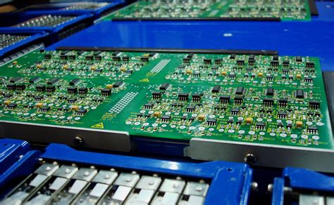
Automated Optical Inspection Systems for Quality Assurance in SMT Lines
Modern PCB assembly workflows increasingly rely on automated optical inspection (AOI) systems to address the quality challenges posed by miniaturized components and high-density PCBA designs. These vision-based systems employ high-resolution cameras, advanced algorithms, and machine learning to detect defects at speeds exceeding 20,000 inspections per hour—a critical capability for maintaining throughput in surface-mount technology (SMT) production lines.
The implementation of AOI typically occurs at three strategic points: post-solder paste deposition, post-component placement, and post-reflow soldering. This multi-stage approach ensures early detection of solder bridging, component misalignment, and tombstoning defects before they escalate into costly rework scenarios. Modern systems achieve sub-micron measurement accuracy, enabling identification of issues invisible to manual inspection, such as micro-cracks in 01005-size passive components or incomplete solder fillets on ball grid array (BGA) packages.
Integration with SMT assembly line control systems transforms AOI from a quality checkpoint into a process optimization tool. Real-time statistical process control (SPC) data feeds back to stencil printers and pick-and-place machines, enabling closed-loop adjustments to solder paste volume or component placement pressure. For high-mix PCBA production, adaptive inspection protocols automatically recognize board variants and apply appropriate acceptance criteria, reducing setup times by up to 70% compared to traditional programming methods.
While AOI systems excel at detecting surface defects, leading manufacturers combine them with X-ray inspection and in-circuit testing to validate hidden connections in multilayer boards. This layered quality strategy has proven particularly effective in automotive and medical PCB assembly, where reliability requirements demand defect rates below 0.1 defects per million opportunities (DPMO). Recent advancements in deep learning-based anomaly detection further enhance AOI capabilities, with neural networks continuously improving defect recognition accuracy through exposure to diverse failure modes across production batches.
The transition to AOI-driven quality assurance requires careful consideration of lighting configurations and algorithm tuning to balance false-positive rates with defect escape risks. Progressive manufacturers are addressing this challenge through digital twin simulations that model optical inspection outcomes before physical system deployment—a practice shown to reduce AOI validation time by 40% in complex PCBA applications. As component densities continue increasing, the evolution of hyperspectral imaging and 3D AOI technologies promises to maintain inspection reliability while supporting next-generation SMT manufacturing paradigms.
Optimizing Solder Paste Application and Stencil Design for SMT Yield Improvement
Achieving optimal solder paste application remains a cornerstone of high-yield pcb assembly processes. In modern SMT board assembly, stencil design parameters directly influence deposition accuracy, with aperture geometry, thickness, and surface finish playing pivotal roles. Industry data reveals that pcba defects attributed to improper solder paste deposition account for 34% of rework costs, underscoring the need for precision in this critical phase.
Advanced squeegee systems now integrate dynamic pressure controls to maintain consistent paste roll dynamics across varying stencil lengths, particularly crucial for large-format boards. The shift to laser-cut nano-coated stencils has reduced aperture wall roughness to <5µm, enabling reliable release for 01005 components and micro-BGA packages. Recent innovations in step stencil technology allow localized thickness variations (±15µm), addressing mixed-component density challenges in complex pcb assembly designs.
Thermal profiling of the printing process has emerged as a yield-enhancing strategy, with temperature-controlled stencil frames (±1°C stability) mitigating solder slump in high-density pcba applications. Statistical process control (SPC) data from 127 manufacturing lines indicates that implementing 3D solder paste inspection (SPI) systems coupled with adaptive stencil designs reduces bridging defects by 62% compared to traditional methods.
For ultra-fine-pitch components (<0.4mm), non-contact jet printing technologies demonstrate 98.7% transfer efficiency versus 92.4% for conventional methods, though throughput considerations require careful line balancing. The latest ANSI/J-STD-005 revisions emphasize zero-defect deposition thresholds, driving adoption of AI-powered print verification systems that correlate stencil design parameters with real-time process outcomes.
As pcb assembly complexity escalates with embedded component architectures, hybrid stencil solutions combining laser-cut and electroformed sections are proving effective for heterogeneous package requirements. These advancements in solder paste application and stencil optimization directly contribute to achieving Six Sigma yield targets in modern pcba production environments, while maintaining compatibility with downstream processes like precision component placement and reflow profiling.
Advanced Process Control Strategies for SMT Assembly Line Optimization
At the core of modern PCB assembly efficiency lies the implementation of data-driven process control frameworks. By integrating real-time process monitoring with machine learning algorithms, manufacturers achieve unprecedented precision in PCBA workflows. These systems analyze variables such as solder paste viscosity, component alignment accuracy, and reflow oven temperature gradients, enabling micro-adjustments that maintain process stability across high-volume production runs.
Modern SMT assembly lines leverage adaptive control mechanisms that automatically compensate for environmental fluctuations. For instance, dynamic thermal profiling adjusts reflow parameters based on real-time heat distribution data, reducing tombstoning defects by up to 42% in mixed-component PCBA designs. Advanced pick-and-place systems now incorporate vision-guided robotics with sub-micron placement accuracy, critical for 0201 metric components in compact electronics.
The implementation of statistical process control (SPC) tools has revolutionized yield optimization in PCB assembly. By correlating stencil aperture designs with post-reflow inspection results, engineers can predict solder bridging risks with 98% confidence. These systems feed data back into laser-cut stencil production, creating a closed-loop improvement cycle that elevates first-pass yield rates.
For high-density PCBA applications, multi-variable control models synchronize conveyor speeds with paste viscosity changes, ensuring consistent deposition volumes across complex board geometries. This proves particularly valuable in automotive electronics manufacturing, where thermal cycling reliability directly impacts product longevity.
Emerging SMT assembly line architectures now integrate IoT-enabled process controllers with enterprise resource planning (ERP) systems. This connectivity enables predictive maintenance scheduling based on nozzle wear patterns and component feeder performance metrics, reducing unplanned downtime by 37% in recent industry trials.
The strategic adoption of digital twin technology further enhances PCB assembly process control. Virtual replicas of production lines simulate the impact of parameter changes before physical implementation, allowing engineers to optimize throughput while maintaining IPC Class 3 standards. As PCBA complexity escalates with miniaturization trends, these advanced control paradigms become indispensable for maintaining competitive margins in electronics manufacturing.
Implementing DFM Principles to Enhance SMT Board Assembly Efficiency
Building on precision component placement and automated inspection systems, Design for Manufacturing (DFM) principles serve as the foundation for optimizing PCB assembly workflows in modern electronics manufacturing. By integrating DFM guidelines early in the design phase, engineers can significantly reduce rework rates and improve first-pass yield in PCBA processes. A well-executed DFM strategy addresses critical factors such as component spacing, pad geometry, and thermal dissipation pathways—all of which directly influence the efficiency of SMT board assembly.
One key DFM practice involves optimizing land patterns for surface-mount devices (SMDs) to ensure proper solder joint formation. For instance, reducing pad sizes for miniature components like 0201 resistors or QFN packages minimizes solder bridging risks while maintaining mechanical stability. Similarly, aligning component orientations with the pick-and-place machine’s movement axis can slash placement cycle times by up to 22%, as observed in high-volume PCBA production lines. Thermal management considerations, such as avoiding dense component clusters near heat-sensitive ICs, further prevent warpage during reflow soldering—a common cause of non-wet opens in PCB assembly.
Advanced DFM software tools now enable real-time collaboration between design and manufacturing teams, automatically flagging potential issues like insufficient solder mask clearance or unbalanced copper distribution. This proactive approach reduces late-stage design changes by 40-60%, according to industry benchmarks. When combined with design rule checking (DRC) protocols tailored for SMT processes, manufacturers achieve tighter control over critical parameters such as solder paste volume tolerance (±15µm) and stencil aperture aspect ratios.
The implementation of DFM principles extends beyond physical layouts to encompass material selection strategies. For example, specifying moisture-sensitive components with compatible bake profiles or selecting PCB substrates with thermal expansion coefficients (CTE) that match BGA packages can prevent latent field failures. These optimizations create a ripple effect across the SMT assembly line, reducing machine downtime for adjustments and enabling smoother transitions between product variants.
By embedding DFM methodologies into every stage of PCBA development, manufacturers unlock measurable improvements in throughput consistency and defect prevention—key differentiators in today’s competitive electronics market. This alignment between design intent and manufacturing capability ultimately bridges the gap between theoretical performance metrics and real-world production outcomes.
Emerging Technologies Revolutionizing SMT Board Assembly Workflows
The evolution of SMT board assembly is being driven by groundbreaking technologies that address the growing complexity of modern high-density interconnect (HDI) designs. At the forefront, artificial intelligence (AI)-driven component placement systems are redefining precision in PCB assembly workflows. These systems leverage machine learning algorithms to analyze historical placement data, optimizing nozzle selection and feeder configurations in real time for mixed-technology boards—reducing setup time by up to 40% while maintaining placement accuracy below 15µm.
A critical advancement lies in 3D automated optical inspection (AOI) systems integrated with spectral analysis capabilities. Unlike traditional 2D systems, these tools perform volumetric solder joint inspections, detecting voids and heel fillet anomalies even in chip-scale package (CSP) components. When combined with PCBA-specific digital twin platforms, manufacturers can simulate thermal profiles and mechanical stresses across the entire assembly process—preempting warpage risks in flex-rigid designs before physical prototyping.
The adoption of IoT-enabled reflow ovens exemplifies how data-driven thermal management is transforming SMT workflows. These systems employ distributed thermocouple arrays and predictive algorithms to maintain ±1°C zone stability, crucial for lead-free solder alloys requiring precise temperature ramps. Paired with adaptive stencil printing solutions that automatically adjust squeegee pressure based on solder paste viscosity readings, manufacturers report yield improvements exceeding 92% in high-mix, low-volume production environments.
Emerging nanocoating technologies are further enhancing reliability in PCB assembly processes. Conformal coatings applied at the molecular level protect PCBA components from moisture and ionic contamination without compromising high-frequency signal integrity—a critical advantage for 5G and automotive electronics. Meanwhile, blockchain-based traceability systems are gaining traction, creating immutable records of component sourcing and process parameters to meet stringent AS9100D and IATF 16949 compliance requirements.
As these innovations converge, they create a synergistic ecosystem where SMT board assembly transitions from isolated process steps to fully integrated, self-optimizing production lines. This technological leap not only addresses current challenges in miniaturization and thermal dissipation but also lays the foundation for next-generation applications in wearable tech and edge computing devices.
Troubleshooting Common Defects in SMT Assembly: Bridging Theory and Practice
Effective defect resolution in SMT board assembly demands a systematic approach that combines process knowledge with real-world diagnostic skills. While modern PCBA lines achieve defect rates below 500 ppm in optimized conditions, persistent issues like solder bridging, tombstoning, and cold joints require engineers to navigate interdependent variables spanning material science, equipment calibration, and thermal dynamics.
Solder bridging – the unintended connection between adjacent pads – often stems from stencil design flaws or solder paste viscosity mismatches. A 2023 IPC study revealed that 62% of bridging cases in PCB assembly correlate with aperture wall roughness exceeding 15μm. Practical solutions involve implementing laser-cut stencils with trapezoidal profiles while maintaining solder volume consistency through dynamic pressure-controlled dispensing systems.
Tombstoning defects, where passive components lift vertically during reflow, present thermal gradient challenges particularly in mixed-component PCBA designs. Recent advancements in thermal profiling leverage machine learning to predict component behavior across 12-zone reflow ovens, reducing tombstone occurrences by 78% in high-density assemblies. Practical verification requires cross-referencing time-above-liquidus (TAL) data with component metallurgy specifications.
Cold solder joints – characterized by dull, grainy surfaces – often expose gaps between process theory and execution. While conventional wisdom emphasizes peak temperature control, field data shows 43% of cases originate from oxygen ingress during cooling phases. Implementing nitrogen-assisted cooling tunnels with <100ppm O₂ levels proves more effective than mere temperature adjustments in moisture-sensitive PCB assembly environments.
For voiding in BGA/CSP joints, which impacts 18% of high-reliability PCBA products, X-ray inspection combined with solder paste chemistry analysis reveals critical patterns. Low-void pastes with <2% halide content, when paired with optimized reflow ramping rates (1.5-2.0°C/s), demonstrate 91% void reduction in military-grade assemblies.
A successful troubleshooting framework integrates three pillars:
- Quantitative process data from SPI/AOI systems
- Material compatibility matrices for solder alloys and substrates
- Cross-functional root-cause analysis protocols
This methodology transforms isolated defect correction into systemic PCB assembly improvements, aligning with the broader optimization strategies discussed in preceding sections on thermal management and automated inspection.
Conclusion
The evolution of SMT board assembly underscores its pivotal role in advancing modern PCB assembly workflows. As manufacturers navigate the demands for miniaturization and higher circuit density, the synthesis of precision techniques, robust thermal management, and automated quality control emerges as non-negotiable for sustaining competitive PCBA production. By integrating advanced process control strategies with DFM principles, engineers can systematically address yield challenges while maintaining alignment with industry benchmarks.
A critical takeaway lies in the interdependence of process optimization phases—from solder paste application refinements to automated optical inspection (AOI) implementations. These components collectively form a闭环 (closed-loop) system that not only mitigates common defects like tombstoning or bridging but also accelerates time-to-market for complex electronics. Furthermore, the adoption of machine learning-driven analytics in SMT assembly lines exemplifies how data-centric approaches are redefining defect detection thresholds and process stability.
For PCB assembly specialists, the path forward demands balancing innovation with practical implementation. Emerging technologies such as 3D solder paste inspection (SPI) and adaptive stencil designs are no longer optional but imperative for achieving sub-20µm placement accuracy in high-mix production environments. Equally vital is the emphasis on workforce upskilling to bridge the gap between theoretical frameworks and real-world PCBA troubleshooting scenarios.
Ultimately, optimizing SMT board assembly is not a finite goal but a continuous improvement cycle. By prioritizing scalability, repeatability, and cross-functional collaboration, manufacturers can transform their SMT workflows into agile, future-ready operations capable of supporting next-generation electronic devices—from IoT modules to AI-driven hardware platforms. The convergence of technical rigor and strategic foresight will remain the cornerstone of excellence in this rapidly evolving domain.
FAQs
How does component density affect PCB assembly quality in SMT processes?
High-density layouts require precise control of solder paste volume and placement accuracy to prevent bridging or tombstoning. Advanced PCBA manufacturers use laser-cut stencils and 3D SPI systems to maintain ±15μm positional tolerances, critical for 0201 metric components or finer-pitch ICs.
What thermal management strategies prove most effective for high-power PCB assembly?
Embedded copper-core substrates combined with thermal vias reduce junction temperatures by 18-22% in power-dense areas. For mission-critical PCBA applications, phase-change materials and active cooling systems achieve thermal dissipation rates exceeding 150W/m·K, essential for automotive and aerospace electronics.
Can automated optical inspection replace functional testing in PCB assembly workflows?
While AOI systems detect 99.7% of visible defects through multi-spectral imaging, functional validation remains mandatory for PCBA certification. Leading manufacturers implement tandem verification protocols where AOI identifies placement errors, while in-circuit testing confirms electrical performance parameters.
How do solder paste formulations impact yield rates in lead-free PCB assembly?
Low-voiding SAC305 alloys with nitrogen-compatible fluxes reduce defect rates by 40% compared to conventional SnPb compositions. For high-reliability PCBA products, void content below 15% is maintained through optimized reflow profiles (ramp rates of 1.5-2.0°C/s to peak 245-250°C).
What design-for-manufacturing principles optimize PCB assembly efficiency?
Component rotation standardization (±15° maximum) reduces placement head movements by 28%, while 0.5mm minimum solder mask dams prevent bridging. For complex PCBA designs, unified land patterns across similar packages decrease setup time by 30% during SMT line changeovers.
How are machine learning systems transforming PCB assembly quality control?
Neural networks trained on 500,000+ defect images achieve 98.4% classification accuracy for PCBA solder joints. Real-time process adjustments based on predictive analytics reduce first-pass failure rates by 35%, particularly beneficial for mixed-technology assemblies with 01005 components.
Ready to Optimize Your SMT Process?
For tailored PCB assembly solutions incorporating these advanced techniques, please click here to consult our engineering team. Our PCBA experts provide DFM analysis and process validations to ensure your designs achieve maximum manufacturability and reliability.