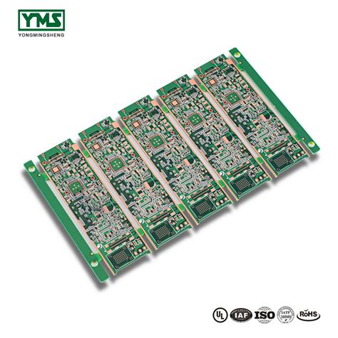
PCB Bare Board Manufacturing Fundamentals

Key Takeaways
Understanding the fundamentals of PCB manufacturing begins with recognizing how core processes influence performance and reliability. When selecting materials for substrate preparation, you’ll need to balance thermal stability, dielectric properties, and mechanical strength—factors that directly affect pcb manufacturing cost and product longevity. For instance, FR-4 epoxy is a common choice, but high-frequency applications may require specialized laminates like Rogers materials.
Conductive layer etching techniques determine circuit precision. Advanced pcb manufacturing companies use photolithography and laser direct imaging to achieve micron-level accuracy, minimizing errors that could escalate costs during mass production. Chemical etching remains a staple, but newer methods like plasma etching are gaining traction for finer trace resolutions.
Tip: Always verify your design’s trace-width-to-current ratios before etching—this prevents overheating and ensures compliance with industry standards like IPC-6012.
When evaluating pcb manufacturing business strategies, prioritize quality assurance testing protocols. Automated optical inspection (AOI) and X-ray testing identify defects in vias or solder masks early, reducing scrap rates. Partnering with certified manufacturers, such as Andwin PCBA, ensures adherence to ISO 9001 and other regulatory frameworks, which is critical for high-reliability sectors like aerospace or medical devices.
Finally, innovations like additive manufacturing and embedded components are reshaping pcb manufacturing, offering faster prototyping and reduced material waste. Whether you’re optimizing for pcb manufacturing cost or scalability, staying updated on these advancements ensures your designs remain competitive in a rapidly evolving market.
Substrate Material Selection Essentials
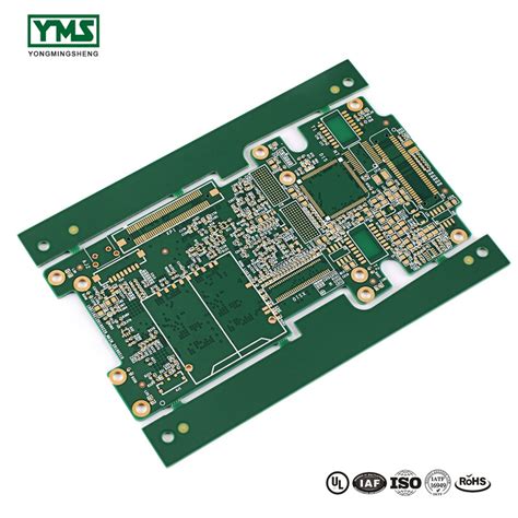
Choosing the right substrate material forms the backbone of successful PCB manufacturing, directly influencing performance, durability, and pcb manufacturing cost. When selecting materials, you’ll encounter options like FR-4, polyimide, and Rogers substrates, each with distinct thermal, mechanical, and electrical properties. For standard applications, FR-4 remains the go-to choice due to its balance of affordability and reliability. However, high-frequency or high-temperature environments often demand specialized materials like ceramic-filled laminates or flexible substrates, which prioritize signal integrity and heat dissipation.
Your decision must align with the end-use requirements of the board. For instance, pcb manufacturing companies serving aerospace or medical industries typically opt for low-loss materials to minimize signal distortion, even if it raises production expenses. Conversely, consumer electronics may prioritize cost-efficiency, leveraging standard substrates without compromising basic functionality. Key parameters to evaluate include dielectric constant (Dk), glass transition temperature (Tg), and coefficient of thermal expansion (CTE)—each impacting how the board behaves under operational stress.
Material thickness also plays a critical role. Thinner substrates enable compact designs but may sacrifice mechanical stability, while thicker options enhance durability at the expense of flexibility. Partnering with experienced pcb manufacturing business providers ensures access to material databases and expert guidance, helping you navigate trade-offs between performance and pcb manufacturing cost. Additionally, consider environmental factors: halogen-free or recyclable substrates are gaining traction as industries adopt greener practices.
Ultimately, substrate selection isn’t just about technical specs—it’s about aligning material properties with your project’s priorities. A misstep here can cascade into issues during conductive layer etching or surface finishing, underscoring why this phase demands meticulous attention. By balancing functional needs with budgetary constraints, you lay a robust foundation for the entire manufacturing process.
Conductive Layer Etching Techniques
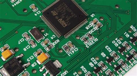
When designing a printed circuit board, PCB manufacturing relies heavily on precise conductive layer etching to create functional circuitry. This process determines how copper traces form connections between components, directly impacting signal integrity and overall performance. Modern PCB manufacturing companies typically employ two primary etching methods: subtractive etching and additive patterning.
In subtractive etching, a copper-clad laminate is coated with a photoresist layer, which is then exposed to UV light through a photomask. After developing the resist, the unprotected copper areas are removed using chemical etchants like ferric chloride or ammonium persulfate. This method balances PCB manufacturing cost and precision, though material waste can accumulate with complex designs.
| Etching Method | Material Efficiency | Typical Use Case |
|---|---|---|
| Subtractive Etching | Moderate | High-volume production |
| Additive Patterning | High | Fine-line, HDI boards |
Additive techniques, such as pattern plating, deposit copper only where needed, reducing waste and enabling finer trace widths (below 3 mil). While this approach lowers long-term PCB manufacturing business expenses by conserving materials, it requires advanced equipment and stricter process control, which may increase upfront costs.
You’ll need to consider factors like etch rate uniformity and undercut control to avoid inconsistencies in trace geometry. Over-etching can narrow conductive paths, raising resistance, while under-etching risks short circuits. Advanced PCB manufacturing companies now use laser-direct imaging (LDI) to improve alignment accuracy, minimizing errors that escalate PCB manufacturing cost during rework.
Environmental regulations also influence technique selection. Many firms transition to alkaline etchants from ferric chloride to meet wastewater disposal standards, ensuring compliance without sacrificing etch quality.
As you optimize etching parameters—such as etchant concentration, temperature, and spray pressure—you’ll balance speed and precision. For multilayer boards, desmear treatments after drilling ensure clean via walls before secondary etching, maintaining conductivity across layers.
Innovations like semi-additive processes (SAP) are gaining traction in high-density interconnect (HDI) PCB manufacturing, allowing ultra-fine traces while keeping material usage efficient. By aligning your process with these advancements, you can enhance yield rates and adapt to evolving industry demands.
Precision Drilling for PCB Vias
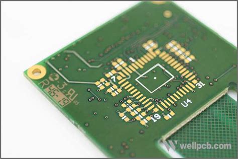
Achieving precise via formation is critical in pcb manufacturing, as these microscopic holes establish electrical connectivity between conductive layers. When working with pcb manufacturing companies, you’ll find that drilling accuracy directly impacts signal integrity and thermal management. Modern processes employ computer-controlled drilling systems to create vias as small as 0.1mm in diameter, requiring tolerances within ±0.025mm.
The choice between mechanical drilling and laser ablation depends on design complexity and pcb manufacturing cost considerations. Mechanical drills, using carbide bits, remain cost-effective for standard through-hole vias. However, UV or CO2 lasers are preferred for high-density interconnects (HDIs) or microvias, enabling finer geometries without compromising substrate integrity.
Drill speed, spindle RPM, and tool wear monitoring are vital to prevent smear formation or burring, which can degrade plating quality. Advanced pcb manufacturing business operations integrate automated optical inspection (AOI) systems to detect deviations in hole placement or wall roughness. For multilayer boards, stacked or staggered via configurations are optimized to balance signal loss and space utilization.
Environmental factors like temperature stability and dust control further influence drilling precision. Leading manufacturers deploy vibration-dampened platforms and real-time thermal compensation to maintain consistency across batches. This attention to detail ensures compliance with IPC-6012 standards while minimizing material waste—a key factor in managing pcb manufacturing cost for high-volume orders.
As you transition to subsequent stages like metallization, remember that improperly drilled vias can cascade into plating voids or delamination. Partnering with certified pcb manufacturing companies that prioritize drill parameter optimization helps mitigate such risks, ensuring your bare boards meet performance benchmarks from prototype to mass production.
Surface Finish Application Methods
Selecting the appropriate surface finish is critical in PCB manufacturing, as it directly impacts performance, durability, and cost. Electroless Nickel Immersion Gold (ENIG) remains a popular choice for high-reliability applications due to its flat surface and wire-bonding capabilities. For PCB manufacturing companies targeting cost-sensitive projects, Hot Air Solder Leveling (HASL) provides a budget-friendly option, though it may struggle with fine-pitch components.
For high-density interconnects, Immersion Silver (IAg) offers excellent conductivity, while Organic Solderability Preservative (OSP) serves as a cost-effective solution for short-lifecycle products. Advanced methods like Electroless Nickel Electroless Palladium Immersion Gold (ENEPIG) are gaining traction in high-frequency applications.
PCB manufacturing costs vary significantly based on finish choice. For instance, ENIG adds ~15-20% to base costs but enhances durability, while HASL remains the most economical. Selective finishes, where multiple finishes are applied to a single board, can optimize PCB manufacturing business margins by balancing performance and cost.
Quality validation involves cross-sectional analysis and thermal cycling to ensure adhesion and solderability. Advanced PCB manufacturing companies now integrate automated optical inspection (AOI) to detect finish inconsistencies. As miniaturization accelerates, alternative finishes like immersion tin or selective gold are gaining traction for high-density designs.
By aligning finish selection with design requirements and end-use conditions, PCB manufacturing achieves the ideal balance of performance, durability, and PCB manufacturing cost efficiency.
Quality Assurance Testing Protocols
When dealing with PCB manufacturing, rigorous quality assurance (QA) protocols ensure your boards meet performance benchmarks while minimizing defects. These protocols begin with automated optical inspection (AOI), which scans for surface-level flaws like incomplete etching or misaligned layers. For internal inspections, X-ray imaging verifies multilayer alignment and identifies hidden voids in vias—critical for high-density designs.
Electrical testing forms the backbone of QA, where continuity checks confirm circuit integrity and isolation tests detect micro-shorts between traces. PCB manufacturing companies often employ flying probe testers for prototype validation, while mass production relies on custom fixture testing to balance speed and accuracy. Environmental stress screening, including thermal cycling and humidity exposure, simulates real-world conditions to weed out boards prone to early failure.
Balancing PCB manufacturing cost with quality requires strategic sampling. Statistical process control (SPC) analyzes defect patterns to pinpoint process inefficiencies, allowing you to adjust parameters before full-scale production. Advanced facilities integrate machine learning to predict failure hotspots, reducing scrap rates by up to 30%.
For a sustainable PCB manufacturing business, compliance with IPC-6012 and ISO 9001 isn’t optional—it’s a competitive differentiator. Documentation trails, from material certifications to final test logs, protect against liability while building client trust. Remember: consistent QA isn’t just about catching flaws; it’s about refining every stage of fabrication to deliver boards that exceed reliability expectations.
Industry Standard Compliance Requirements
When engaging in PCB manufacturing, adhering to industry standards isn’t optional—it’s a cornerstone of building trust and ensuring reliability. Regulatory bodies like IPC (Association Connecting Electronics Industries), UL (Underwriters Laboratories), and ISO (International Organization for Standardization) define stringent criteria for PCB manufacturing companies to follow. These standards govern everything from material purity to dimensional accuracy, ensuring your bare boards meet global performance benchmarks.
For example, IPC-6012 specifies requirements for rigid PCBs, including copper thickness tolerances and hole-wall integrity, while ISO 9001 mandates robust quality management systems. Compliance reduces risks of defects, minimizes PCB manufacturing cost overruns from rework, and safeguards your reputation in competitive markets. Ignoring these protocols could lead to failed inspections, delayed shipments, or even legal liabilities—especially when supplying industries like aerospace or medical devices.
To stay compliant, you’ll need documented evidence of process controls, such as material certifications and traceability records. Third-party audits are common, requiring PCB manufacturing business operators to maintain transparent workflows. This includes validating etching precision through cross-section analysis or using automated optical inspection (AOI) systems to detect micro-cracks.
Balancing compliance with efficiency requires strategic planning. While stricter standards may raise initial costs, they often lower long-term expenses by reducing waste and warranty claims. Partnering with certified suppliers and investing in employee training ensures consistency, keeping your operations aligned with evolving regulations like REACH for hazardous substances or RoHS for lead-free materials.
Ultimately, meeting industry standards isn’t just about avoiding penalties—it’s about delivering boards that perform reliably under stress, fostering long-term client relationships, and positioning your business as a leader in quality-driven PCB manufacturing.
Advanced Manufacturing Process Innovations
As the electronics industry evolves, pcb manufacturing companies are adopting cutting-edge technologies to address rising complexity and efficiency demands. Laser direct imaging (LDI) systems now replace traditional photolithography, enabling micron-level precision in circuit patterning while reducing material waste. This shift not only enhances yield rates but also optimizes pcb manufacturing cost by minimizing rework.
Another breakthrough lies in additive manufacturing techniques, such as inkjet printing of conductive traces. Unlike subtractive etching, this method deposits materials only where needed, slashing copper waste by up to 60%. For high-frequency applications, firms are integrating low-loss dielectric substrates with engineered thermal properties, ensuring signal integrity without compromising durability.
Automation plays a pivotal role in modern pcb manufacturing business models. Robotic optical inspection (AOI) systems equipped with AI algorithms detect defects 30% faster than manual checks, critical for maintaining ISO 9001 compliance. Meanwhile, IoT-enabled predictive maintenance monitors drilling spindles and plating baths in real time, cutting unplanned downtime by 22%.
Environmental sustainability is reshaping processes too. Companies now deploy halogen-free laminates and lead-free surface finishes to meet RoHS directives, while closed-loop water recycling systems reduce effluent discharge by 45%. These innovations align with cost-reduction strategies, as greener practices often correlate with long-term pcb manufacturing savings through tax incentives and reduced liability risks.
To stay competitive, you’ll need to evaluate hybrid manufacturing approaches that combine rigid and flexible board fabrication in a single workflow. This method eliminates connector dependencies in compact designs, directly impacting assembly time and product reliability. By leveraging these advancements, manufacturers can deliver higher-value solutions while navigating fluctuating material costs and tighter industry regulations.
Conclusion
As you navigate the complexities of PCB manufacturing, it becomes clear that every stage—from substrate preparation to final inspection—directly impacts the reliability and performance of electronic systems. While PCB manufacturing companies employ advanced technologies to optimize processes, understanding the fundamentals empowers you to make informed decisions when selecting partners or evaluating production methods.
The balance between PCB manufacturing cost and quality remains a critical consideration. By prioritizing precision in conductive layer etching and durability in surface finishes, you ensure boards meet both functional requirements and industry standards. Innovations like automated optical inspection (AOI) and laser drilling have redefined efficiency, but their implementation depends on a manufacturer’s technical expertise and equipment investments.
For businesses operating in the PCB manufacturing business, aligning with suppliers who adhere to ISO and IPC standards minimizes risks of defects and delays. You’ll also want to assess scalability—whether a partner can accommodate evolving designs or shifts in material preferences without compromising turnaround times.
Ultimately, the success of your project hinges on transparency across the supply chain. Request detailed documentation on quality assurance protocols and material traceability, especially when working with high-frequency or high-density designs. As PCB manufacturing evolves with trends like additive processes and eco-friendly substrates, staying informed ensures your choices future-proof both prototypes and mass-produced boards.
This becomes particularly evident when analyzing lifecycle costs: opting for cheaper, short-term solutions might reduce initial PCB manufacturing cost, but could lead to higher failure rates downstream. By contrast, investing in robust manufacturing practices strengthens product longevity, reinforcing your reputation in competitive markets.
FAQs
How does substrate material selection impact overall PCB manufacturing costs?
The choice of substrate material directly influences PCB manufacturing cost due to variations in thermal stability, dielectric properties, and mechanical strength. High-frequency applications often require specialized laminates, which can increase expenses compared to standard FR-4 materials.
What should you look for when choosing among PCB manufacturing companies?
Prioritize firms with certifications like ISO 9001 and IPC-A-600 to ensure adherence to industry standard compliance requirements. Additionally, evaluate their expertise in conductive layer etching techniques and access to advanced equipment for precision drilling and surface finish application.
Can prototyping affect the scalability of a PCB manufacturing business?
Yes. Prototyping phases help identify design flaws early, reducing costly revisions during mass production. Reputable PCB manufacturing companies often offer scalable solutions, balancing low-volume prototyping with high-volume production capabilities to support business growth.
How do quality assurance protocols influence reliability in PCB manufacturing?
Rigorous testing methods—such as automated optical inspection (AOI) and electrical testing—ensure defects like short circuits or misaligned vias are caught before shipment. These protocols minimize field failures, protecting your PCB manufacturing business from reputational and financial risks.
What innovations are reshaping advanced PCB manufacturing processes?
Technologies like laser direct imaging (LDI) and additive manufacturing enable finer trace widths and faster turnaround times. Such advancements help PCB manufacturing companies meet evolving demands for miniaturized, high-performance boards while optimizing PCB manufacturing cost.
Ready to Optimize Your PCB Production?
For tailored solutions in PCB manufacturing, explore our advanced capabilities and competitive pricing. Please click here to consult with our experts and streamline your next project.