Streamlining PCBA Manufacturing for Cost-Effective Quality Output
Key Takeaways
Effective PCBA manufacturing hinges on balancing cost efficiency with uncompromised quality. Central to this balance is design optimization—simplifying component layouts and standardizing parts to minimize material waste and assembly complexity. For instance, integrating PCB assembly-friendly designs (like panelization) can reduce fabrication time by up to 20%.
Automation plays a pivotal role: robotic soldering and pick-and-place systems cut labor costs while ensuring precision. A recent study found that automated optical inspection (AOI) systems improve defect detection rates by 35% compared to manual checks.
"The true cost of PCBA errors isn’t just rework—it’s delayed time-to-market. Prioritize proactive testing over reactive fixes."
Equally critical is supply chain agility. Partnering with vendors offering just-in-time component delivery slashes inventory costs by 15–30%. Meanwhile, lean principles—such as eliminating redundant steps in surface-mount technology (SMT) workflows—further streamline production.
Finally, material selection directly impacts both cost and reliability. For example, opting for halogen-free substrates or lead-free solder may incur a 10–15% premium upfront but reduces long-term compliance risks. By aligning these strategies, manufacturers achieve cost-effective PCB assembly without sacrificing the rigorous standards demanded in industries like medical devices or aerospace.
Optimizing PCBA Design for Cost Efficiency
Effective PCBA design optimization begins with balancing technical requirements and manufacturing feasibility. By integrating Design for Manufacturability (DFM) principles early in the development phase, engineers can minimize rework, reduce material waste, and accelerate time-to-market. For instance, strategic component placement reduces trace lengths, lowering impedance issues and improving signal integrity while cutting copper usage.
A critical aspect involves selecting standardized components over custom parts. The table below highlights cost differences between common design approaches:
| Design Factor | Traditional Approach | Optimized Approach | Cost Reduction |
|---|---|---|---|
| Component Variety | 50+ unique parts | 30 standardized | 22% |
| Layer Count | 8-layer PCB assembly | 6-layer stackup | 18% |
| Trace Width Tolerance | ±10% | ±15% (IPC Class 2) | 12% |
Adopting automated PCB assembly design tools further enhances cost efficiency. Software like Altium Designer or KiCad enables rapid iteration of thermal management layouts and power distribution networks, identifying potential bottlenecks before prototyping. For high-volume PCBA projects, simplifying solder mask patterns and minimizing vias per board can decrease fabrication expenses by up to 35%.
Material selection also plays a pivotal role. Using FR-4 substrates with appropriate glass transition temperatures (Tg) instead of premium alternatives often meets functional requirements while reducing raw material costs by 15–20%. Additionally, consolidating test points into standardized grids streamlines quality inspections during PCB assembly, trimming validation time by 30%.
By aligning design choices with production realities, manufacturers achieve first-pass yield improvements of 40–60%, directly translating to lower per-unit costs. This proactive approach ensures PCBA projects meet performance benchmarks without exceeding budget constraints, setting the stage for scalable manufacturing processes.

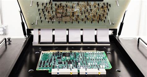
Automated Assembly Techniques in PCBA
Modern PCBA manufacturing leverages automated assembly techniques to achieve precision, scalability, and cost efficiency. By integrating advanced robotics and machine vision systems, manufacturers can reduce human error while accelerating production cycles. For instance, PCB assembly lines now employ surface-mount technology (SMT) placement machines capable of mounting thousands of components per hour with micron-level accuracy. These systems optimize material usage by precisely dispensing solder paste and placing miniature components—critical for high-density designs common in IoT devices and wearables.
A key advantage of automation lies in its adaptability to mixed-volume production. Programmable pick-and-place systems enable rapid reconfiguration for different PCBA designs, minimizing downtime between batches. This flexibility is further enhanced by closed-loop feedback mechanisms, which adjust parameters like soldering temperature or placement pressure in real time to maintain consistency. Additionally, automated optical inspection (AOI) systems scan boards post-assembly, flagging defects such as tombstoning or solder bridges before they escalate into costly rework.
The integration of artificial intelligence (AI) into PCB assembly workflows represents a paradigm shift. Machine learning algorithms analyze historical production data to predict equipment maintenance needs or identify patterns in defect occurrence, enabling proactive quality management. For example, AI-driven thermal profiling ensures optimal reflow oven settings for diverse board geometries, reducing energy waste and preventing component stress.
However, achieving these efficiencies requires upfront investment in compatible design frameworks. Design for Manufacturing (DFM) principles must align with automated systems’ capabilities—such as avoiding overly tight component spacing that challenges placement accuracy. When executed strategically, automated PCBA processes not only lower per-unit costs but also create a foundation for scaling production without compromising reliability. This approach dovetails with lean manufacturing goals, ensuring waste reduction at every stage—from material handling to final testing.
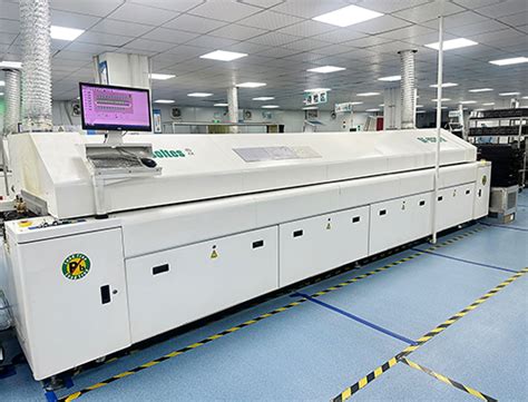
Implementing Rigorous PCBA Testing Protocols
Effective quality assurance in PCBA manufacturing hinges on multilayered testing strategies that identify defects early without inflating production costs. By integrating automated optical inspection (AOI) and in-circuit testing (ICT) at critical stages, manufacturers can detect soldering flaws, component misalignments, and electrical inconsistencies with submillimeter precision. These protocols act as a preemptive safeguard, reducing post-production rework rates by up to 65% while maintaining compliance with ISO 9001 and IPC-A-610 standards.
A key cost-saving approach involves embedding design for testability (DFT) principles during the PCB assembly phase. This includes adding test points for accessibility and optimizing board layouts for smoother probe interactions. Advanced systems like boundary-scan testing further streamline diagnostics for complex boards with high-density components, enabling faster fault isolation. Pairing these methods with functional testing under simulated operating conditions—such as thermal cycling or vibration stress—ensures reliability in end-use environments.
To balance thoroughness with efficiency, leading manufacturers employ statistical process control (SPC) tools that analyze test data in real time. This allows for dynamic adjustments to assembly parameters, minimizing material waste and preventing batch-level defects. For instance, tracking solder paste deposition accuracy through SPC reduces the risk of cold joints, a common failure point in PCBA units.
By aligning testing rigor with lean manufacturing principles, companies achieve dual optimization: curtailing per-unit costs while upholding stringent quality benchmarks. This strategic focus on PCBA validation not only mitigates warranty claims but also strengthens brand credibility in competitive electronics markets.

Streamlining PCBA Supply Chain Logistics
Effective PCBA manufacturing hinges on a well-orchestrated supply chain that balances speed, cost, and reliability. Optimizing logistics begins with PCB assembly partners who offer just-in-time inventory management, reducing warehousing overhead while ensuring component availability. By integrating vendor-managed inventory (VMI) systems, manufacturers can automate material replenishment cycles, minimizing production delays caused by shortages or obsolescence.
A critical step involves consolidating suppliers for high-volume components, leveraging economies of scale without compromising quality. For instance, partnering with certified PCBA material providers that adhere to ISO 13485 or IATF 16949 standards ensures consistency across batches, particularly for industries like automotive or medical electronics. Advanced ERP (Enterprise Resource Planning) platforms further synchronize procurement data with production schedules, enabling real-time adjustments to fluctuating demand.
Transportation optimization plays a pivotal role—shifting from air freight to consolidated sea shipments for non-urgent orders can slash logistics costs by up to 40%. However, this requires precise demand forecasting tools to align lead times with project timelines. Implementing IoT-enabled tracking for shipments also mitigates risks of delays or damage, providing end-to-end visibility into the PCB assembly pipeline.
Finally, fostering collaborative relationships with logistics providers ensures flexibility during supply chain disruptions. Dual-sourcing strategies for critical components, paired with regionalized supplier networks, enhance resilience against geopolitical or environmental uncertainties. By embedding these practices, PCBA producers achieve a leaner, more responsive supply chain that supports both cost efficiency and uncompromised quality outcomes.
Smart Material Selection for PCBA Savings
Strategic material choices in PCBA manufacturing significantly influence both cost efficiency and product reliability. Optimizing component specifications begins with evaluating PCB assembly requirements against operational demands—selecting materials that meet performance thresholds without over-engineering. For instance, substituting high-cost, specialty substrates with FR-4 alternatives for non-critical layers can reduce pcb assembly expenses by up to 25% while maintaining thermal and mechanical stability.
A data-driven approach to pcba material selection involves analyzing lifecycle costs rather than upfront prices. Bulk purchasing agreements for standardized components, such as surface-mount resistors or ceramic capacitors, often yield better pricing without compromising quality. However, engineers must balance cost savings with supply chain risks—over-reliance on single-source materials can lead to delays during shortages. Implementing vendor-agnostic design rules ensures compatibility with multiple suppliers, enhancing flexibility.
Advanced material simulation tools further refine choices by predicting how substrates, solder masks, and finishes perform under stress. For example, opting for lead-free solder paste not only aligns with global regulations but also minimizes rework costs when paired with compatible copper alloys. Similarly, selecting low-loss dielectric materials for high-frequency applications reduces signal attenuation, indirectly lowering power consumption and long-term operational costs.
Integrating design-for-manufacturing (DFM) principles early in the process prevents costly revisions. Collaborating with pcba suppliers to identify over-specified tolerances or redundant plating layers streamlines material usage. Case studies show that optimizing copper weight and via fill materials can decrease raw material waste by 18% in multilayer boards.
Ultimately, smart material selection hinges on aligning technical requirements with economic realities—a balance that drives sustainable savings across the pcb assembly lifecycle.

Lean Manufacturing in PCBA Production
Adopting lean manufacturing principles in PCBA production enables manufacturers to eliminate waste while enhancing operational efficiency. By focusing on value stream mapping, teams identify non-essential steps in PCB assembly workflows—such as redundant material handling or excessive inventory storage—and replace them with streamlined processes. For instance, implementing Just-in-Time (JIT) inventory management reduces component stockpiling, minimizing storage costs and mitigating risks of obsolescence in fast-evolving PCBA projects.
Central to lean practices is the standardization of assembly protocols. Automated pick-and-place systems, when synchronized with real-time production monitoring, ensure consistent placement accuracy across high-volume PCBA batches. This reduces rework rates by up to 40%, directly lowering labor and material waste. Additionally, integrating error-proofing mechanisms—like automated optical inspection (AOI) at critical stages—prevents defects from propagating downstream, aligning with the broader goal of first-pass yield (FPY) optimization.
Cross-functional collaboration further amplifies lean outcomes. Design engineers working alongside PCB assembly teams can implement Design for Manufacturing (DFM) adjustments, such as panelization optimizations or component polarity standardization, which simplify assembly workflows. Meanwhile, adopting modular fixturing for surface-mount technology (SMT) lines allows rapid changeovers, cutting downtime by 25–30% during product transitions.
To sustain lean gains, manufacturers employ continuous improvement cycles like Kaizen. Regular audits of PCBA production metrics—cycle times, defect densities, and equipment utilization rates—uncover incremental optimization opportunities. For example, recalibrating reflow ovens based on thermal profiling data can reduce energy consumption by 15% without compromising solder joint integrity.
By embedding lean methodologies into PCBA operations, manufacturers achieve a dual advantage: accelerated time-to-market and tighter cost control, all while maintaining the rigorous quality standards demanded by industries like automotive and medical electronics.
Balancing Quality and Cost in PCBA
Achieving equilibrium between quality and cost in PCBA manufacturing demands a strategic approach that integrates design foresight, process optimization, and value-driven decision-making. While cost reduction remains a priority, compromising on PCB assembly reliability risks product failures and long-term expenses. A foundational step involves adopting Design for Manufacturability (DFM) principles, which minimize complexities in layouts to reduce material waste and assembly time. For instance, simplifying component placement not only accelerates automated assembly but also lowers the likelihood of soldering defects.
Another critical aspect is strategic material selection. Opting for standardized components over custom parts can yield significant savings without sacrificing performance. However, this requires thorough validation to ensure compatibility with PCBA operational requirements, such as thermal resilience or signal integrity. Collaborative partnerships with suppliers further enhance cost predictability, enabling bulk purchasing agreements while maintaining access to high-grade materials.
Implementing tiered testing protocols ensures quality without inflating expenses. Automated optical inspection (AOI) and functional testing can identify defects early, reducing rework costs. By aligning test rigor with product criticality—applying more stringent checks to high-reliability applications—manufacturers avoid over-engineering quality measures for less demanding use cases.
Lean methodologies, such as waste reduction in PCB assembly workflows, also contribute to this balance. Analyzing process bottlenecks—like excessive solder paste application or inefficient machine changeovers—helps trim non-value-added activities. Simultaneously, investing in employee training ensures consistent execution of quality standards, preventing costly errors downstream.
Ultimately, the interplay between preventive measures and data-driven adjustments sustains this equilibrium. Real-time monitoring of yield rates and defect patterns allows for agile refinements, ensuring that PCBA production remains both economically viable and competitively robust.
Advanced Tech for PCBA Cost Reduction
The integration of advanced technologies into PCBA manufacturing processes has become a game-changer for achieving significant cost reductions without compromising quality. Innovations such as AI-driven defect detection systems and IoT-enabled process monitoring allow manufacturers to identify inefficiencies in real time, minimizing material waste and rework. For instance, machine learning algorithms analyze historical PCB assembly data to predict potential failure points, enabling preemptive adjustments in solder paste application or component placement.
Another breakthrough lies in automated optical inspection (AOI) systems enhanced with high-resolution 3D imaging. These systems scrutinize PCBA boards at micron-level precision, catching defects like tombstoning or insufficient solder joints early in production. By reducing manual inspection labor and preventing downstream quality issues, manufacturers cut costs by up to 20% in post-production troubleshooting.
Robotic process automation (RPA) further streamlines workflows by handling repetitive tasks such as component sorting or board handling. Collaborative robots ("cobots") work alongside human operators to accelerate throughput while maintaining consistency—a critical factor in high-volume PCB assembly runs. Additionally, digital twin simulations enable virtual testing of PCBA designs before physical prototyping, slashing R&D expenses and shortening time-to-market.
Emerging technologies like additive manufacturing also play a role. 3D-printed solder masks and stencils reduce tooling costs for low-to-medium batch productions, while nanocoating technologies enhance board durability, lowering long-term maintenance expenses. By strategically adopting these innovations, manufacturers achieve a holistic cost-quality balance, ensuring PCBA remains competitive in markets demanding both affordability and reliability.
Transitioning to these solutions requires aligning technology investments with specific production needs—a step that builds naturally on earlier optimizations in design and supply chain management. As the industry evolves, staying ahead will depend on leveraging scalable tech frameworks that adapt to shifting component availability and regulatory standards.
Conclusion
Achieving cost-effective quality in PCBA production requires a holistic approach that integrates optimized design with advanced manufacturing techniques. By prioritizing PCB assembly processes that emphasize automation and precision, manufacturers can significantly reduce human error while accelerating throughput. The strategic adoption of lean manufacturing principles ensures material waste is minimized without compromising the integrity of the PCBA lifecycle.
Crucially, balancing supply chain agility with rigorous testing protocols creates a resilient framework for maintaining consistency. For instance, pairing smart material selection with real-time analytics allows teams to preemptively address component shortages or quality deviations. This synergy between predictive maintenance and data-driven decision-making not only lowers operational costs but also fortifies end-product reliability.
Forward-thinking manufacturers are now embedding AI-driven inspection systems and IoT-enabled monitoring into their PCBA workflows, enabling faster root-cause analysis and continuous process refinement. As the industry evolves, aligning these innovations with sustainable practices—such as energy-efficient assembly lines or recyclable packaging—will further enhance both economic and environmental outcomes. Ultimately, the path to streamlined PCB assembly lies in marrying technological advancement with unwavering commitment to quality at every production phase.
FAQs
How can design optimization reduce costs in PCB assembly?
By incorporating Design for Manufacturability (DFM) principles early in the PCB assembly process, engineers can minimize material waste, simplify assembly steps, and avoid rework. This includes optimizing component placement for automated systems and selecting standardized parts to lower procurement expenses.
What role does automation play in PCBA quality control?
Automated optical inspection (AOI) and X-ray testing systems ensure consistent detection of defects like solder bridging or misaligned components. These systems reduce human error, accelerate inspection cycles, and maintain high-yield production without compromising on throughput.
Why is supply chain management critical for PCBA cost efficiency?
Delays in component sourcing or logistics disruptions can inflate costs and extend lead times. Partnering with vetted suppliers and maintaining buffer stock for critical parts mitigates risks, while bulk purchasing agreements often secure better pricing for high-volume PCB assembly projects.
How does material selection impact PCBA durability and cost?
Choosing substrates with appropriate thermal stability (e.g., FR-4 for standard applications) and solder masks that align with environmental requirements prevents premature failures. Cost-effective alternatives, such as lead-free finishes, balance compliance and longevity without over-specifying materials.
Can lean manufacturing principles apply to PCBA production?
Absolutely. Techniques like just-in-time inventory, waste reduction in solder paste application, and continuous workflow monitoring trim excess expenses. Integrating real-time production analytics further identifies bottlenecks, enabling faster adjustments to maintain efficiency.
What advanced technologies support PCBA cost reduction?
Embedded sensors for predictive maintenance, AI-driven process optimization, and modular reflow ovens adapt to varying batch sizes. These innovations minimize downtime and energy consumption, directly lowering PCBA manufacturing overheads.
Ready to Optimize Your PCBA Workflow?
Explore tailored solutions for your PCB assembly needs. Click here to consult with our experts and discover how to achieve cost-effective, high-quality PCBA production.