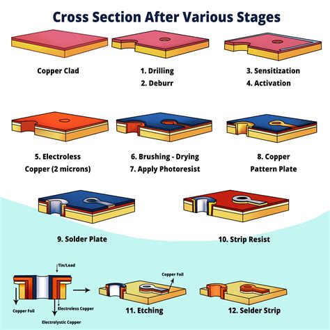
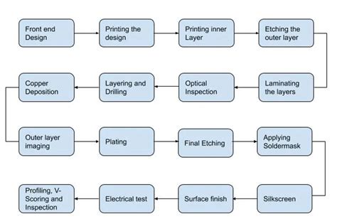
Multilayer PCB Fabrication Process Essentials Explained

Key Takeaways
Understanding the PCB manufacturing process for multilayer boards helps you optimize design choices and avoid costly errors. When working with high-density interconnects or complex stackups, prioritizing precision in layer alignment and thermal management ensures reliable performance. For PCB manufacturing companies, balancing PCB manufacturing cost with quality requires careful material selection and process validation.
"Investing in advanced lamination controls and automated optical inspection (AOI) systems can reduce defects by up to 30% in multilayer PCB manufacturing business operations." – Insights from Andwin PCBA.
Key considerations include:
- Material preparation: Choosing low-loss dielectrics and high-Tg laminates to withstand thermal stress during lamination.
- Via fabrication: Using laser-drilled microvias or staggered plated-through holes (PTHs) to maintain signal integrity in dense layouts.
- Stackup optimization: Aligning impedance-controlled layers and power planes to minimize electromagnetic interference (EMI).
When evaluating PCB manufacturing cost, factor in design complexity, layer count, and testing protocols. For example, adding buried vias or hybrid materials may increase upfront expenses but reduce long-term failure risks. Partnering with experienced PCB manufacturing companies ensures access to specialized expertise, such as sequential lamination techniques or embedded passive components.
To streamline your PCB manufacturing business, implement real-time process monitoring during critical stages like oxide treatment and press cycles. This minimizes layer misalignment and delamination, which account for over 40% of multilayer PCB defects. Always validate designs through simulation tools before prototyping to avoid costly re-spins.
Multilayer PCB Material Preparation Essentials
Proper material selection forms the foundation of successful PCB manufacturing, directly impacting both performance and reliability. High-frequency applications, for instance, demand materials with stable dielectric constants to minimize signal loss. When sourcing materials, PCB manufacturing companies prioritize substrates with low thermal expansion coefficients to withstand thermal cycling during assembly.
Key considerations include the choice of prepreg (pre-impregnated fiberglass) and copper foil thickness. For instance, low-profile copper (≤12µm) enhances fine-line etching for HDI boards, while high-Tg (glass transition temperature) materials ensure stability in high-temperature environments.
A critical yet often underestimated factor is moisture absorption control. Even slight moisture ingress during PCB manufacturing processes can lead to delamination during reflow. Leading PCB manufacturing businesses implement vacuum-sealed packaging and humidity-controlled storage to mitigate this.
Cost drivers in material selection involve balancing performance requirements against PCB manufacturing costs. For instance, while polyimide films offer superior thermal stability, their higher cost may not justify their use in consumer-grade applications. A practical example: A recent project by a leading PCB manufacturing company achieved 15% cost reduction by switching to halogen-free FR-4 alternatives without compromising signal integrity.
Material preparation also extends to surface finishes. While ENIG (Electroless Nickel Immersion Gold) remains popular for its shelf life and solderability, emerging alternatives like ENEPIG (Electroless Nickel Electroless Palladium Immersion Gold) offer superior wire bonding capabilities for advanced packaging.
By aligning material choices with design requirements and production realities, you can optimize both performance and PCB manufacturing costs, ensuring your project remains competitive in high-density interconnect markets.
Precision Layer Alignment Techniques Explained
Achieving micron-level accuracy in layer alignment separates functional multilayer boards from costly manufacturing rejects. You’ll need optical alignment systems with vision-assisted registration to align prepreg layers and copper foils within ±25µm tolerance. Modern pcb manufacturing companies employ laser-guided fiducial markers and automated optical inspection (AOI) to verify alignment before lamination—critical for boards with high-density interconnects (HDIs) or buried vias.
For optimal results, start with stress-relieved core materials to minimize thermal expansion mismatches. Use registration pins compatible with your pcb manufacturing equipment, ensuring consistent tooling hole placement across all layers. When working with 12+ layer stacks, sequential lamination cycles require intermediate alignment checks to correct cumulative errors. Advanced shops combine X-ray layer-to-layer registration with real-time correction algorithms, reducing pcb manufacturing cost by cutting scrap rates by up to 40%.
Don’t overlook the impact of material handling—even slight warping during transport can ruin alignment. Temperature-controlled cleanrooms (22±2°C) paired with vacuum-sealed storage for moisture-sensitive substrates help maintain dimensional stability. For flexible hybrid boards, pcb manufacturing business leaders recommend laser direct imaging (LDI) systems that bypass traditional phototools, achieving <15µm layer-to-layer overlay accuracy.
Transitioning to the next stage, precise alignment directly enables reliable thermal management in multilayer pcbs by ensuring uninterrupted thermal via connections. Misaligned layers create microgaps that trap heat or disrupt ground planes—a critical consideration for high-frequency designs. Always validate alignment against your impedance control specifications before committing to full lamination cycles.
Thermal Lamination Process Control Methods
Achieving consistent results in PCB manufacturing relies heavily on mastering thermal lamination parameters. This stage bonds individual layers into a unified structure while maintaining dimensional stability and dielectric integrity. For PCB manufacturing companies, precise control over temperature, pressure, and dwell time ensures void-free bonding—critical for high-density designs where even minor defects compromise performance.
Start by calibrating heating platens to maintain a uniform temperature gradient. Variations exceeding ±2°C across the press can lead to uneven resin flow, creating weak spots in the bond. Most PCB manufacturing business operations use automated systems to monitor real-time thermal profiles, adjusting for material-specific requirements like the glass transition temperature (Tg) of prepregs.
Pressure management is equally vital. Excessive force squeezes out too much resin, risking delamination during drilling or thermal cycling. Insufficient pressure leaves air pockets that degrade signal integrity. Modern laminators employ closed-loop hydraulic controls, balancing ram force (typically 200-400 psi) with material thickness and layer count.
Dwell time optimization directly impacts PCB manufacturing cost. Over-curing increases energy consumption and cycle times, while under-curing weakens interlayer adhesion. For example, FR-4 materials often require 60-90 minutes at 180°C, but high-speed laminates may need adjusted profiles. Partnering with experienced PCB manufacturing companies helps tailor these parameters to your stackup complexity, avoiding costly reworks.
Post-lamination cooling rates also demand attention. Rapid quenching introduces internal stresses, warping boards and misaligning vias. Gradual cooling (2-4°C/minute) preserves layer registration—a critical factor when aligning 12+ layer boards with microvias.
By integrating sensor-driven process controls and predictive analytics, manufacturers minimize deviations that affect yield. This precision becomes indispensable as designs push toward 20-layer architectures with mixed dielectric materials, where thermal management flaws cascade into field failures.
Next, advanced via fabrication techniques build on this foundation, addressing signal integrity challenges introduced by dense interconnects.
Advanced Via Fabrication for Signal Integrity
Achieving reliable signal transmission in multilayer PCB manufacturing demands meticulous attention to via design and fabrication. Blind vias, buried vias, and microvias each serve distinct roles in optimizing signal paths while minimizing electromagnetic interference (EMI). When working with PCB manufacturing companies, you’ll find that advanced via structures reduce parasitic capacitance and inductance, critical for high-speed digital or RF applications.
The choice of via type directly impacts PCB manufacturing cost. For instance, laser-drilled microvias enable finer pitch designs but require specialized equipment, increasing production expenses. A balanced approach involves analyzing signal frequency, layer count, and thermal requirements early in the design phase. Consider the following comparison:
| Via Type | Typical Diameter | Layer Penetration | Cost Impact |
|---|---|---|---|
| Through-Hole | 0.3–0.5 mm | All layers | Low |
| Blind/Buried | 0.1–0.3 mm | Selective layers | Moderate to High |
| Microvia (Laser) | 0.05–0.15 mm | Adjacent layers | High |
To maintain signal integrity, PCB manufacturing business practices often employ back-drilling to remove unused via stubs, which can cause signal reflections. Additionally, filled vias with conductive epoxy improve thermal dissipation—a key consideration for boards requiring strict thermal management.
Material selection further influences performance. Low-loss dielectrics like Rogers or Isola substrates reduce signal attenuation, while proper via plating (e.g., electroless nickel immersion gold) ensures consistent conductivity. Collaborating with PCB manufacturing partners early helps align design choices with fabrication capabilities, avoiding costly redesigns.
Transitioning from lamination to via formation requires precision. Misaligned vias disrupt impedance continuity, undermining the benefits of optimized stackup designs. By integrating simulation tools and adhering to IPC-2221B standards, you can preemptively address signal degradation risks, ensuring robust performance in mission-critical applications.
Optimizing Circuit Board Stackup Designs
When planning multilayer PCB manufacturing, your stackup configuration directly impacts performance, cost, and reliability. A well-optimized design balances signal integrity with thermal management while accounting for PCB manufacturing cost constraints. Start by analyzing the number of layers required: high-speed designs often demand 8-12 layers for proper impedance control, while simpler applications might function with 4-6.
Key considerations include material selection and dielectric spacing. High-frequency signals require low-loss laminates like Rogers materials, but these increase PCB manufacturing business expenses. For cost-sensitive projects, FR-4 remains a practical base, though hybrid stackups combining premium and standard materials can optimize performance-to-cost ratios. Work closely with PCB manufacturing companies to validate material compatibility with your lamination and drilling processes.
Layer arrangement governs electromagnetic interference (EMI) reduction. Place power and ground planes adjacent to signal layers to create controlled impedance paths and shield sensitive traces. Symmetrical stackups minimize warpage risks during thermal cycling—a critical factor for boards exposed to harsh environments. For example, a 10-layer board might follow this sequence: Signal-Ground-Signal-Power-Signal-Ground-Signal.
Signal integrity optimization requires meticulous trace routing and via placement. Avoid parallel routing of high-speed traces across adjacent layers to prevent crosstalk. Use buried or blind vias in dense designs to conserve space, but remember these advanced via types raise PCB manufacturing cost by 15-25% compared to through-hole variants.
Thermal expansion mismatches between materials remain a hidden challenge. Copper weight variations across layers can create uneven stress during thermal lamination, leading to delamination. Experienced PCB manufacturing partners use simulation tools to predict thermal behavior, adjusting copper distribution and prepreg selection accordingly.
Finally, prototype testing is non-negotiable. Implement TDR (Time Domain Reflectometry) measurements to verify impedance consistency and cross-section microsectioning to inspect layer alignment. These steps ensure your stackup meets both electrical and mechanical tolerances before full-scale production.

Thermal Management in Multilayer PCBs
Effective thermal management becomes critical as you scale circuit complexity in multilayer PCB manufacturing. Heat dissipation challenges intensify with higher layer counts and denser component placement, requiring deliberate design choices to prevent performance degradation or premature failure. Modern PCB manufacturing companies address this by integrating thermal considerations at every stage, from material selection to post-processing.
Start by evaluating substrate materials with higher thermal conductivity ratings, such as polyimide-based laminates or ceramic-filled dielectrics. These materials reduce heat accumulation in inner layers while maintaining signal integrity. For power-hungry designs, increasing copper weight in plane layers (e.g., 2 oz instead of 1 oz) enhances heat spreading—a balance between PCB manufacturing cost and thermal performance.
Strategic via placement plays a dual role: thermal vias beneath high-power components create vertical heat paths to outer heatsinks, while staggered microvia arrays prevent localized hotspots. When planning these structures, consider how lamination pressures and resin flow during fabrication affect via wall integrity. Advanced PCB manufacturing business practices often combine laser-drilled vias with plugging materials like conductive epoxy to optimize thermal and electrical pathways simultaneously.
Layer stackup design directly influences thermal behavior. Alternating high-power and low-power signal layers with ground planes helps distribute heat more evenly. For extreme environments, PCB manufacturing specialists may recommend embedded copper coins or metal-core substrates, though these options require tighter process controls to avoid delamination risks.
Post-fabrication steps like applying thermal interface materials (TIMs) or integrating heatsinks with optimized surface roughness further enhance cooling. Simulation tools such as finite element analysis (FEA) allow you to model thermal gradients before production, reducing iterative prototyping costs—a key advantage when partnering with experienced PCB manufacturing companies.
Always verify thermal management efficacy through infrared imaging during electrical testing. This ensures your design meets both operational reliability standards and economic constraints inherent to PCB manufacturing cost calculations.
Multilayer Board Electrical Testing Protocols
After addressing thermal management and lamination quality, verifying electrical performance becomes critical in PCB manufacturing. Rigorous testing protocols ensure that complex multilayer boards meet design specifications and function reliably under real-world conditions. Automated Optical Inspection (AOI) systems typically perform initial checks for visible defects, but advanced electrical testing is required to validate connectivity, impedance, and signal integrity across all layers.
PCB manufacturing companies rely on two primary methods: bed-of-nails testing for prototype validation and flying probe testing for small-batch production. The former uses custom fixtures to contact test points simultaneously, while the latter employs movable probes for flexible, low-volume verification. Both approaches detect opens, shorts, and resistance mismatches that could compromise board functionality. For high-frequency applications, Time-Domain Reflectometry (TDR) analyzes impedance continuity in critical traces, ensuring signal integrity matches the stackup design.
Balancing PCB manufacturing cost with testing thoroughness requires strategic planning. Implementing boundary scan testing (JTAG) reduces fixture expenses for complex boards by leveraging built-in test circuitry. However, boards with analog components or high-speed interfaces often need supplemental in-circuit testing (ICT), which increases upfront tooling costs but improves fault coverage.
In high-volume PCB manufacturing business operations, combining testing stages optimizes efficiency. Post-lamination testing verifies interlayer connections before drilling, while post-assembly testing validates component integration. Statistical process control (SPC) tools track failure patterns, helping refine fabrication parameters to minimize defects. Modern testing suites also incorporate thermal cycling simulations to identify latent weaknesses in plated through-holes or via structures.
To maintain competitiveness, prioritize testing protocols that align with your board’s complexity and application demands. For aerospace or medical-grade PCBs, 100% electrical testing becomes non-negotiable, whereas consumer electronics might adopt sampling-based approaches. Always document test results meticulously—this data proves invaluable for troubleshooting production issues and demonstrating compliance with industry standards like IPC-6012.
Ensuring Quality in PCB Lamination Stages
Achieving consistent quality during PCB manufacturing lamination requires meticulous control over material behavior and process parameters. Thermal expansion mismatches between prepregs and copper layers can lead to delamination or warpage, particularly in high-layer-count boards. To mitigate this, PCB manufacturing companies prioritize selecting compatible materials with matched coefficients of thermal expansion (CTE) and glass transition temperatures (Tg).
Precise temperature ramping during lamination is critical. Rapid heating risks entrapping volatiles, creating voids, while uneven cooling introduces residual stresses. Modern presses use programmable profiles that adjust heating rates based on the resin system’s gelation characteristics. Pressure distribution must also be optimized—excessive force squeezes out too much resin, weakening interlayer bonds, whereas insufficient pressure fails to eliminate air pockets.
For cost-sensitive projects, PCB manufacturing cost considerations often drive the use of standardized lamination cycles. However, complex designs with mixed dielectric materials or embedded components demand customized profiles. Advanced manufacturers employ real-time pressure sensors and dielectric analysis (DEA) tools to monitor resin flow and cure states, ensuring void-free bonding without over-engineering the process.
Post-lamination inspection methods like ultrasonic scanning or cross-sectional analysis verify layer adhesion quality. These steps are non-negotiable for PCB manufacturing business models targeting aerospace or medical applications, where reliability trumps production speed. Implementing statistical process control (SPC) charts for critical parameters—temperature deviations under ±2°C, pressure uniformity within 5%—helps maintain batch-to-batch consistency.
Transitioning to subsequent drilling or plating stages hinges on flawless lamination outcomes. Even minor voids or misaligned layers amplify signal loss in high-frequency circuits, underscoring why this phase directly impacts both yield rates and long-term board performance.
Conclusion
Navigating the complexities of multilayer PCB fabrication demands a strategic approach that balances technical precision with economic viability. Whether you’re optimizing pcb manufacturing cost or ensuring signal integrity in high-density designs, every decision—from material selection to thermal management—directly impacts the final product’s reliability. For pcb manufacturing companies, mastering advanced techniques like laser-drilled microvias and controlled impedance stacking isn’t optional; it’s a competitive necessity in an industry where miniaturization and performance are paramount.
When evaluating pcb manufacturing business strategies, consider how sequential lamination cycles and automated optical inspection (AOI) systems influence both quality and scalability. While tighter tolerances may raise initial costs, they reduce long-term risks like signal loss or thermal stress—critical factors for applications in aerospace or medical devices. Partnering with experienced pcb manufacturing specialists ensures access to cutting-edge processes like direct imaging or plasma etch, which streamline production timelines without compromising layer alignment accuracy.
Ultimately, the success of your multilayer PCB project hinges on aligning technical requirements with budgetary constraints. By prioritizing material compatibility and stackup symmetry, you mitigate risks associated with delamination or impedance mismatches. For businesses scaling their pcb manufacturing operations, investing in robust testing protocols—such as boundary scan or thermal cycling—builds resilience against field failures while reinforcing brand credibility. In a landscape where innovation drives demand, optimizing these fundamentals positions your designs for both performance excellence and market relevance.
FAQs
What factors influence pcb manufacturing cost for multilayer boards?
Material selection, layer count, and via formation complexity directly affect pcb manufacturing cost. High-density interconnects (HDI) and specialized substrates like FR-4 or polyimide increase expenses, while bulk orders often reduce per-unit pricing.
How do pcb manufacturing companies ensure layer alignment accuracy?
Advanced pcb manufacturing companies use optical registration systems and laser-drilled fiducial markers to achieve micron-level precision. Automated optical inspection (AOI) verifies alignment between inner layer cores and prepreg materials before lamination.
Why is thermal management critical in pcb manufacturing business operations?
Poor heat dissipation risks delamination and signal loss, especially in high-power designs. Leading pcb manufacturing business providers integrate thermal vias, copper balancing, and thermal interface materials to mitigate hotspots and ensure long-term reliability.
Can stackup design impact pcb manufacturing timelines?
Yes, unconventional layer configurations or mixed dielectric materials require additional engineering reviews. Most pcb manufacturing partners recommend standardized stackups to avoid delays, though custom solutions are feasible for specialized applications.
What certifications should you prioritize when selecting pcb manufacturing companies?
Look for ISO 9001, IPC Class 3, and UL certifications. These validate adherence to signal integrity standards and quality control protocols, particularly for mission-critical applications like aerospace or medical devices.
Need Expert Guidance for Your Multilayer PCB Project?
For tailored solutions that balance pcb manufacturing cost and performance, please click here to consult our engineering team. We specialize in optimizing complex designs for manufacturability without compromising reliability.