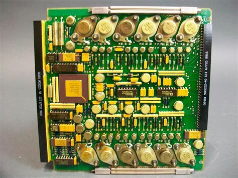
Pcb printed circuit board design high frequency wiring skills
(1) High-frequency circuits are often highly integrated and have high wiring density.
The use of multilayer boards is necessary for wiring and is also an effective means to reduce interference.
(2) The fewer bends in the leads between the pins of high-speed circuit devices, the better.
It is best to use all-straight lines for the leads of high-frequency circuit wiring. If a turn is required, a 45° bend line or arc turn can be used. Meeting this requirement can reduce the external emission of high-frequency signals and mutual coupling.
(3) The shorter the leads between the pins of high-frequency circuit devices, the better.
(4) The fewer inter-layer alternations of the leads between the pins of high-frequency circuit devices, the better. The so-called “the fewer inter-layer alternations of the leads, the better” means that the fewer vias (Via) used in the component connection process, the better. According to measurements, one via can bring about 0.5 pF of distributed capacitance. Reducing the number of vias can significantly increase the speed.

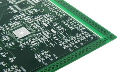
Techniques for high-frequency wiring in PCB design
(5) When wiring high-frequency circuits, attention should be paid to the “cross interference” introduced by the close parallel routing of signal lines.
If parallel distribution cannot be avoided, a large area of ”ground” can be arranged on the opposite side of the parallel signal lines to greatly reduce interference. Parallel routing within the same layer is almost inevitable, but the routing directions of two adjacent layers must be perpendicular to each other.
(6) Measures to enclose particularly important signal lines or local units with ground lines are implemented, that is, the outer contour of the selected object is drawn.
This function can automatically perform the so-called “ground envelopment” treatment on the selected important signal lines. Of course, using this function for local ground envelopment treatment of clock and other units will also be very beneficial for high-speed systems.
(7) All types of signal routing cannot form loops, and ground lines cannot form current loops.
(8) A high-frequency decoupling capacitor should be set near each integrated circuit block.
(9) When analog ground lines, digital ground lines, etc. are connected to the common ground line, a high-frequency choke link should be used.
In the actual assembly of high-frequency choke links, high-frequency ferrite beads with wires passing through the center holes are often used. They are generally not expressed in the circuit schematic, and the resulting network table (netlist) does not include such components, so their existence will be ignored during wiring. In view of this reality, it can be treated as an inductor in the schematic diagram, and a component package can be defined for it separately in the PCB component library. Before wiring, it can be manually moved to a suitable position close to the common ground point.
(10) Analog circuits and digital circuits should be arranged separately. After independent wiring, the power supply and ground should be connected at a single point to avoid mutual interference.
(11) Before the DSP, off-chip program memory and data memory are connected to the power supply, a filter capacitor should be added and placed as close to the chip power pin as possible to filter out power supply noise. In addition, it is recommended to shield around key parts such as the DSP and off-chip program memory and data memory to reduce external interference.
(12) The off-chip program memory and data memory should be placed as close to the DSP chip as possible, and the
layout should be reasonable so that the length of the data line and the address line are basically the same. In particular, when there are multiple memories in the system, the distance from the clock line to the clock input of each memory should be equal, or a separate programmable clock driver chip can be added. For the DSP system, an external memory with an access speed similar to that of the DSP should be selected, otherwise the high-speed processing capability of the DSP will not be fully utilized. The DSP instruction cycle is in the nanosecond level, so the most common problem in the DSP hardware system is high-frequency interference. Therefore, when making the printed circuit board (PCB) of the DSP hardware system, special attention should be paid to the correct and reasonable wiring of important signal lines such as address lines and data lines. When wiring, try to make the high-frequency line short and thick, and stay away from signal lines that are susceptible to interference, such as analog signal lines. When the circuits around the DSP are more complex, it is recommended to make the DSP and its clock circuit, reset circuit, off-chip program memory, and data memory into a minimum system to reduce interference.
(13) When following the above principles and mastering the skills of using design tools, after manual wiring is completed, high-frequency circuits generally need to be simulated using advanced PCB simulation software in order to improve the reliability and manufacturability of the system.
Due to space limitations, this article does not provide a detailed introduction to specific simulations, but it is recommended that if conditions permit, the system must be simulated. Here are a few basic concepts.
Let me give you a basic explanation.
What are electromagnetic interference (EMI) and electromagnetic compatibility (EMC)?
Electromagnetic interference (Electromagnetic Interference) has two types: conducted interference and radiated interference. Conducted interference refers to the coupling (interference) of a signal on an electrical network to another electrical network through a conductive medium. Radiated interference refers to the coupling (interference) of an interference source to another electrical network through space. In high-speed PCB and system design, high-frequency signal lines, integrated circuit pins, various connectors, etc. may become radiated interference sources with antenna characteristics, which can emit electromagnetic waves and affect the normal operation of other systems or other subsystems within the system.
What is signal integrity?
Signal integrity refers to the quality of the signal on the signal line. Good signal integrity means that the signal has the necessary voltage level value when it is needed. Poor signal integrity is not caused by a single factor, but by multiple factors in board-level design. The main signal integrity problems include reflection, oscillation, ground bounce, crosstalk, etc.
What is reflection?
Reflection is the echo on the transmission line. Part of the signal power (voltage and current) is transmitted to the line and reaches the load, but part of it is reflected. If the source and load have the same impedance, reflection will not occur. Impedance mismatch between the source and load will cause reflection on the line, and the load will reflect part of the voltage back to the source. If the load impedance is less than the source impedance, the reflected voltage is negative, and vice versa, if the load impedance is greater than the source impedance, the reflected voltage is positive. Changes in wiring geometry, improper line termination, transmission through connectors, and discontinuities in power planes can all cause such reflections.
What is crosstalk?
Crosstalk is the coupling between two signal lines. The mutual inductance and mutual capacitance between the signal lines cause noise on the line. Capacitive coupling causes coupling current, while inductive coupling causes coupling voltage. PCB layer parameters, signal line spacing, electrical characteristics of the driver and receiver, and line termination methods all have a certain impact on crosstalk.
What are overshoot and undershoot?
Overshoot is the first peak or valley that exceeds the set voltage – the highest voltage for the rising edge and the lowest voltage for the falling edge. Undershoot refers to the next valley or peak. Excessive overshoot can cause the protection diode to work, resulting in premature failure. Excessive undershoot can cause false clock or data errors (misoperation).
What are ringing and rounding?
The phenomenon of ringing is repeated overshoot and undershoot. Signal ringing and rounding are caused by excessive inductance and capacitance on the line. Ringing is underdamped and rounding is overdamped. Signal integrity problems usually occur in periodic signals, such as clocks. Ringing and rounding are caused by multiple factors like reflections. Ringing can be reduced by proper termination, but it is impossible to completely eliminate it.
What is ground plane bounce noise and reflux noise?
When there is a large current surge in the circuit, ground plane bounce noise (referred to as ground bounce) will be caused. For example, when the outputs of a large number of chips are turned on at the same time, a large transient current will flow through the power plane of the chip and the board. The inductance and resistance of the chip package and the power plane will cause power noise, which will cause voltage fluctuations and changes on the real ground plane (0V). This noise will affect the operation of other components. The increase in load capacitance, the decrease in load resistance, the increase in ground inductance, and the increase in the number of switching devices will all lead to an increase in ground bounce.
Due to the division of the ground plane (including power and ground), for example, the ground layer is divided into digital ground, analog ground, shielding ground, etc., when the digital signal goes to the analog ground area, ground plane reflux noise will be generated. Similarly, the power layer may also be divided into 2.5V, 3.3V, 5V, etc. Therefore, in multi-voltage PCB design, the bounce noise and reflux noise of the ground plane need to be paid special attention.
What is the difference between the time domain and the frequency domain?
The time domain is the process of voltage or current changes based on time, which can be observed with an oscilloscope. It is often used to find pin-to-pin delays, skew, overshoot, undershoot, and settling time.
The frequency domain is the process of voltage or current changes based on frequency, which can be observed with a spectrum analyzer. It is often used to compare waveforms with FCC and other EMI control limits.
What is impedance?
Impedance is the ratio of input voltage to input current on a transmission line (Z0=V/I). When a source sends a signal to the line, it will hinder it from driving it until 2*TD, where TD is the delay of the line.
What is settling time?
Settling time is the time required for an oscillating signal to settle to a specified final value.
What is pin-to-pin delay?
Pin-to-pin delay is the time between a change in state at the driver and a change in state at the receiver. These changes usually occur at 50% of a given voltage, with the minimum delay occurring when the output first crosses a given threshold and the maximum delay occurring when the output is the last to cross the voltage threshold, all measured in this case.
What is skew?
The skew of a signal is the difference in time between the arrival of the same net at different receivers. Skew is also used to describe the difference in time between the arrival of clock and data at a logic gate.
What is slew rate?
The slew rate is the slope of an edge (the ratio of the time change of a signal’s voltage). I/O specifications (such as PCI) state between two voltages, which is the slew rate, and it can be measured.
What is a quiescent line?
It does not switch during the current clock cycle. Also called a “stuck-at” line or static line. Crosstalk can cause a quiescent line to switch during a clock cycle.
What is false clocking?
False clocking means that the clock changes state unconsciously after crossing the threshold (sometimes between VIL or VIH). It is usually caused by excessive undershoot or crosstalk.
What is an IBIS model?
The IBIS (Input/Output Buffer Information Specification) model is a method for quickly and accurately modeling I/O BUFFER based on the V/I curve. It is an international standard that reflects the chip driver and receiver electrical characteristics. It provides a standard file format to record parameters such as drive source output impedance, rise/fall time and input load, which is very suitable for calculation and simulation of high-frequency effects such as oscillation and crosstalk.
IBIS itself is just a file format. It explains how to record different parameters of a chip driver and receiver in a standard IBIS file, but does not explain how to use these recorded parameters. These parameters need to be read by the simulation tool using the IBIS model. To use IBIS for actual simulation, you need to complete the following four tasks first.
(1) Obtain the original source of information about chip drivers and receivers;
(2) Obtain a method to convert the original data into IBIS format;
(3) Provide layout and routing information that can be recognized by computers for simulation;
(4) Provide a software tool that can read IBIS and layout and routing formats and perform analytical calculations.
IBIS is a simple and intuitive file format that is well suited for circuit simulation tools similar to Spice (but not Spice, because the IBIS file format cannot be directly read by Spice tools). It provides a description of the behavior of drivers and receivers without revealing the intellectual property details of the internal structure of the circuit. In other words, vendors can use IBIS models to illustrate their latest gate-level design work without revealing too much product information to their competitors. And, because IBIS is a simple model, when doing a simple load simulation, it saves 10 to 15 times the calculation amount than the corresponding full Spice transistor-level model simulation.
IBIS provides two complete V-I curves representing the driver in the high and low states, as well as the state transition curve at a certain conversion speed. The function of the V-I curve is to provide IBIS with the ability to model nonlinear effects such as protection diodes, TTL totem pole drive sources, and emitter follower outputs.
What is a SPICE model?
SPICE is the abbreviation of Simulation Program with Integrated Circuit Emphasis.
Hardware debugging skills
Some issues that should be paid attention to during hardware debugging. For example, before hardware debugging, the circuit board should be carefully inspected to see if there is a short circuit or open circuit (since the PCB wiring of the DSP is generally dense and thin, the probability of this happening is still relatively high). After powering on, use your hands to feel whether some chips are particularly hot. If it is found that some chips are very hot, you need to immediately turn off the power and recheck the circuit. After troubleshooting, you should then check whether the crystal is oscillating and whether the reset is correct and reliable. Then use an oscilloscope to check whether the signals of the CLK-OUT1 and CLK-OUT2 pins of the DSP are normal. If normal, it means that the DSP itself is basically working normally.
(1) Ensure the stability and reliability of the power supply
Before debugging the DSP hardware system, you should ensure that the power supply for the experimental board has good constant voltage and constant current characteristics. It is particularly important to note that the DSP input voltage should be maintained at 5.0V±0.05V. If the voltage is too low, an error message will appear when writing the program to the Flash through the JTAG interface; if the voltage is too high, the DSP chip will be damaged.
(2) Use simulation software to eliminate hardware faults
After completing the inspection of the circuit board, you can debug the program through the simulation software. Since the program code is downloaded to the off-chip program memory in the target system during simulation, some hardware faults can be easily checked through simulation software.
After power-on, if the simulation software debugging window cannot load the program, there are two possibilities:
① The DSP chip pins are open or short-circuited;
② The DSP chip is damaged. If this is the first time to Use simulation software to debug the program. At this time, the experimental board should be powered off and the welding of each pin of the DSP chip should be carefully checked.
If the software debugging window has correctly loaded the program, the DSP chip may be damaged. At this time, the impedance of the entire board of the experimental board can be detected to further determine whether the DSP chip is damaged. If the impedance of the entire board drops sharply, the power line that supplies power to the DSP chip can be cut off to detect the resistance of the DSP chip.
If the software debugging window can load the program, but the loaded program is partially wrong, such as the code for operating the off-chip program memory or data memory becomes .word xxxx, then the off-chip program memory or data memory may be faulty. The memory should be carefully checked for short circuits or cold soldering. If not, it should be further determined whether the memory is damaged.