Working principle and composition of circuit boards
Working principle and composition of circuit boards
Circuit boards can be called printed circuit boards or printed circuit boards. The English names are (Printed Circuit Board) PCB, (Flexible Printed Circuit board) FPC circuit boards (FPC circuit boards are also called flexible circuit boards. Flexible circuit boards are made of polyimide or polyester film as substrates. A highly reliable and extremely flexible printed circuit board. The names of circuit boards include: ceramic circuit boards, alumina ceramic circuit boards, aluminum nitride ceramic circuit boards, circuit boards, PCB boards, aluminum substrates, high-frequency boards, thick copper boards, impedance boards, PCBs, ultra-thin circuit boards, ultra-thin circuit boards, printed (copper etching technology) circuit boards, etc.
1.Working principle
The working principle of the circuit board is to use the board base insulating material to isolate the surface copper foil conductive layer, so that the current flows along the pre-designed route in various components to complete functions such as work, amplification, attenuation, modulation, demodulation, encoding, etc.
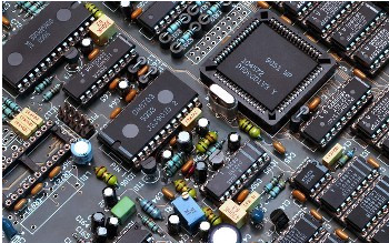
Figure 1 Circuit board
2.Composition
The circuit board is mainly composed of pads, vias, mounting holes, wires, components, connectors, filling, electrical boundaries, etc. The main functions of each component are as follows:
Pads: metal holes for soldering component pins.
Via: There are metal vias and non-metal vias, among which metal vias are used to connect component pins between layers.
Mounting holes: used to fix the circuit board.
Wire: electrical network copper film used to connect component pins.
Connectors: components used to connect between circuit boards.
Filling: copper used for ground network, which can effectively reduce impedance.
Electrical boundary: used to determine the size of the circuit board, and all components on the circuit board cannot exceed this boundary.
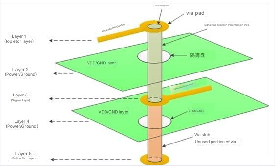
Figure 2 Via structure of circuit board
3.Classification
Circuit boards are divided into three major categories according to the number of layers: single-sided board, double-sided board, and multi-layer circuit board.
Multilayer board: refers to a printed board with more than three layers of conductive graphic layers and insulating materials in between, and the conductive graphics in between are interconnected as required. Multilayer circuit boards are the product of the development of electronic information technology towards high speed, multi-function, large capacity, small size, thinness, and lightness.
Single-sided board: On the most basic PCB, parts are concentrated on one side and wires are concentrated on the other side. Because the wires only appear on one side, this PCB is called a single-sided circuit board. Single-sided boards are usually simple to make and low in cost, but the disadvantage is that they cannot be applied to too complex products.
Double-sided board: It is an extension of single-sided board. When single-layer wiring cannot meet the needs of electronic products, double-sided boards must be used. Both sides have copper cladding and routing, and the lines between the two layers can be connected through vias to form the required network connection.
According to the characteristics, circuit boards are divided into flexible circuit boards (FPC), rigid circuit boards (PCB), and flexible and rigid combined circuit boards (FPCB).
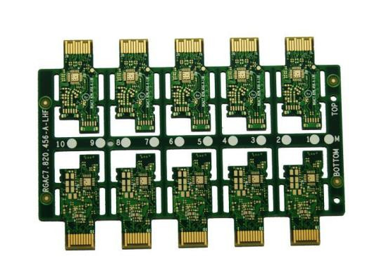
Figure 3 Multilayer circuit board
4.Working layer
The circuit board includes many types of working layers, such as signal layer, protective layer, silk screen layer, internal layer, etc. The functions of various layers are briefly introduced as follows:
(1) Protective layer: mainly used to ensure that the places on the circuit board that do not need tinning are not tinned, thereby ensuring the reliability of the circuit board operation. Among them, Top Paste and Bottom Paste are the top solder mask layer and the bottom solder mask layer respectively; Top Solder and Bottom Solder are the solder paste protective layer and the bottom solder paste protective layer respectively.
(2) Signal layer: mainly used to place components or wiring. Protel DXP usually contains 30 middle layers, namely Mid Layer1~Mid Layer30. The middle layer is used to arrange signal lines, and the top and bottom layers are used to place components or copper.
(3) Silkscreen layer: mainly used to print the serial number, production number, company name, etc. of components on the circuit board.
(4) Internal layer: mainly used as a signal wiring layer. Protel DXP contains a total of 16 internal layers.
(5) Other layers: mainly include 4 types of layers.
Drill Guide: mainly used for the location of drilling holes on the printed circuit board.
Keep-Out Layer: mainly used to draw the electrical frame of the circuit board.
Drill Drawing: mainly used to set the drilling shape.
Multi-Layer: mainly used to set multi-layer.
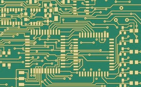
Figure 4 Circuit board working layer
This article introduces the concept, working principle, composition, classification and working level of the circuit board. Depending on the design of the circuit board, the price will be determined by the material of the circuit board, the number of layers of the circuit board, the size of the circuit board, the quantity produced each time, the production process, the minimum line width and line spacing, the minimum hole diameter and the number of holes, special process requirements and other requirements.