Optimizing PCB Assembly: Precision Engineering for Manufacturing Excellence

Key Takeaways
Effective PCB assembly (PCBA) relies on a synergy of precision engineering and rigorous quality control to achieve manufacturing excellence. At its core, optimizing PCB assembly processes involves minimizing variability while maximizing repeatability—critical for producing high-performance electronic devices. Modern manufacturers prioritize automated optical inspection (AOI) and surface-mount technology (SMT) to ensure component placement accuracy, reducing defects by up to 40% in high-volume production.
A key focus lies in streamlining workflows, where lean manufacturing principles eliminate bottlenecks and reduce cycle times. For instance, integrating design for manufacturability (DFM) checks during the prototyping phase prevents costly rework by aligning board layouts with assembly capabilities. Additionally, thermal management strategies, such as optimized reflow soldering profiles, enhance solder joint reliability—a critical factor in devices exposed to extreme operating conditions.
Cost efficiency remains inseparable from quality in PCBA. Adopting advanced material selection (e.g., high-Tg substrates) and predictive maintenance for pick-and-place machinery lowers long-term operational costs while sustaining yield rates. Moreover, real-time data analytics enable proactive adjustments, ensuring process parameters align with evolving design requirements.
Finally, traceability systems embedded within PCB assembly lines safeguard compliance with industry standards like IPC-A-610, reinforcing product reliability. By harmonizing these strategies, manufacturers not only elevate manufacturing efficiency but also future-proof their operations against emerging technological demands.

PCB Assembly Precision Engineering
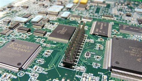
Precision engineering forms the backbone of modern PCB assembly processes, where micrometer-level accuracy directly impacts the functionality of electronic devices. At the heart of PCBA (Printed Circuit Board Assembly) lies the meticulous alignment of components, solder paste application, and reflow soldering—each requiring advanced machinery calibrated to nanometer-level tolerances. Automated pick-and-place systems, for instance, now achieve placement accuracies of ±25 microns, ensuring surface-mount devices (SMDs) adhere to design specifications without compromising signal integrity.
Tip: To maintain consistency in high-density PCB assembly, implement real-time thermal profiling during reflow soldering. This minimizes voids in solder joints and prevents component warping under thermal stress.
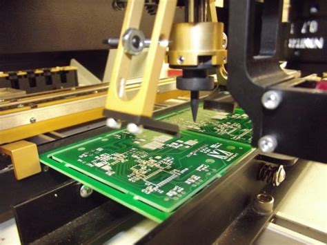
The integration of laser-assisted inspection tools has revolutionized quality assurance in PCBA workflows. These systems detect defects such as tombstoning or solder bridging with 99.98% accuracy, far exceeding traditional manual checks. Furthermore, the adoption of 3D solder paste inspection (SPI) ensures optimal volume and alignment before component placement, reducing rework rates by up to 60%. For mission-critical applications—like aerospace or medical electronics—PCB assembly protocols often incorporate six-sigma methodologies to limit defect densities to fewer than 0.1 defects per million opportunities (DPMO).
Material selection also plays a pivotal role in precision engineering. High-temperature laminates and low-loss dielectrics are increasingly paired with controlled-impedance routing to mitigate signal attenuation in high-frequency designs. As miniaturization trends push trace widths below 50µm, PCBA providers must balance geometric precision with thermal management strategies, such as embedding microvias or using thermally conductive underfills.
By aligning design-for-manufacturing (DFM) principles with precision-driven PCB assembly techniques, manufacturers can achieve repeatable outcomes even for complex, multilayer boards with 0201-sized components. This synergy between engineering rigor and advanced manufacturing tools ensures that modern electronics meet both performance benchmarks and reliability expectations in demanding operational environments.
Quality Control in PCB Manufacturing
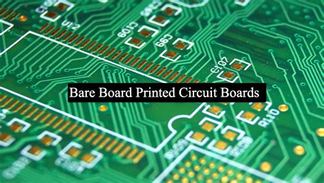
Effective PCB assembly relies on rigorous quality control protocols to ensure the reliability and performance of electronic devices. Modern manufacturing facilities employ automated optical inspection (AOI) systems to detect microscopic defects in solder joints, component placement accuracy, and trace integrity during PCBA processes. These systems, combined with X-ray inspection for hidden connections in ball grid array (BGA) components, create a multi-layered verification framework that minimizes human error.
Statistical process control (SPC) methodologies further enhance quality by analyzing production data in real time, identifying trends that could indicate potential deviations in PCB assembly parameters such as reflow oven temperatures or paste application consistency. Manufacturers adhering to ISO 9001 and IPC-A-610 standards implement traceability systems that log material batch numbers, machine calibration records, and operator signatures for each PCBA unit—a critical feature for industries requiring compliance with aerospace or medical device regulations.
To address evolving challenges like miniaturization and high-density interconnects, advanced labs now integrate environmental stress testing into quality workflows. Thermal cycling tests simulate years of operational wear in hours, while vibration testing validates solder joint durability in automotive or industrial applications. This proactive approach to PCB assembly quality not only reduces field failure rates but also aligns with zero-defect manufacturing philosophies that prioritize lifecycle reliability over short-term cost savings.
Transitioning seamlessly into streamlined processes, these quality measures form the foundation for optimizing manufacturing efficiency without compromising the precision demanded by modern electronics.
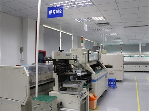
Streamlining PCB Assembly Processes
Efficient PCB assembly relies on systematically refining workflows to eliminate bottlenecks while maintaining stringent quality standards. Modern high-mix, low-volume production environments demand agile processes that balance speed with precision. A critical first step involves implementing automated optical inspection (AOI) systems to identify defects in solder paste application or component placement before reflow soldering. This reduces rework rates by up to 40% while preserving material integrity.
Central to streamlining PCBA workflows is the adoption of lean manufacturing principles. By mapping value streams across surface-mount technology (SMT) lines, manufacturers can minimize non-productive intervals between stencil printing and final testing. Real-time production monitoring systems further enhance throughput by providing actionable data on machine utilization rates and cycle times. For instance, integrating smart conveyor systems that automatically adjust transport speeds based on downstream equipment availability prevents component jams and reduces idle time.
Process standardization proves vital when scaling PCB assembly operations. Developing unified work instructions for solder paste storage, stencil cleaning frequencies, and reflow oven profiling ensures consistent output across multiple production shifts. Advanced factories now employ digital twin simulations to model thermal dynamics during soldering, enabling preemptive adjustments that prevent warping or cold joints.
Material management innovations contribute significantly to streamlined PCBA manufacturing. Just-in-time component delivery systems synchronized with pick-and-place machines reduce inventory costs by 18-25% while preventing production delays. Moreover, implementing cross-functional training programs equips technicians with skills to handle both SMT and through-hole assembly tasks, creating flexible teams capable of adapting to rapid design changes.
These optimization strategies create a foundation for implementing more sophisticated techniques discussed in subsequent sections, ensuring PCB assembly efficiency improvements align with broader manufacturing excellence goals.
Advanced PCB Assembly Techniques
Modern PCB assembly processes leverage precision engineering to address the growing complexity of electronic devices. PCBA (Printed Circuit Board Assembly) now integrates automated optical inspection (AOI) systems and 3D solder paste inspection (SPI) to achieve micron-level accuracy in component placement. These technologies reduce human error by 60–75% compared to manual methods, particularly in high-density interconnect (HDI) designs.
| Technique | Application Scope | Yield Improvement |
|---|---|---|
| Laser Direct Imaging | Fine-line circuitry (<25µm) | 12–18% |
| Selective Soldering | Mixed-component boards | 20–25% |
| Embedded Component | RF/microwave applications | 30–35% |
The adoption of intelligent thermal profiling ensures optimal solder joint formation across PCB assembly stages. Advanced reflow ovens with closed-loop nitrogen control maintain oxygen levels below 50 ppm, minimizing oxidation during PCBA processes. For mission-critical applications, automated x-ray inspection (AXI) detects hidden defects in ball grid array (BGA) packages with 99.98% accuracy.
Material science innovations further enhance these techniques. Low-loss dielectric substrates and halogen-free solder masks now enable PCBA systems to operate reliably at 5G/mmWave frequencies. Concurrently, machine learning algorithms analyze production data in real time, predicting potential failures 8–12 hours before they occur.
To maintain competitiveness, manufacturers combine these advanced PCB assembly techniques with design for manufacturing (DFM) principles. This synergy reduces rework cycles by 40% while improving signal integrity in multi-layer boards. As IoT and AI applications demand smaller, faster electronics, such integrated engineering approaches will remain pivotal in achieving manufacturing excellence.
Cost-Effective PCB Manufacturing Solutions
Achieving cost-effective PCB manufacturing solutions requires balancing precision engineering with strategic resource allocation. A critical starting point is optimizing PCB assembly workflows to minimize material waste and reduce cycle times. By leveraging design for manufacturability (DFM) principles, engineers can simplify layouts to lower PCBA complexity, directly cutting production costs without compromising functionality. For instance, standardizing component footprints and reducing the number of unique parts in a bill of materials (BOM) streamlines procurement and minimizes inventory overhead.
Material selection also plays a pivotal role. Transitioning to high-yield substrates or adopting panelized board designs maximizes raw material utilization, particularly in high-volume PCB assembly runs. Additionally, partnering with suppliers offering bulk pricing for commonly used ICs or passive components can yield substantial savings. Advanced manufacturers further enhance cost efficiency by integrating automated optical inspection (AOI) systems early in the PCBA process, identifying defects before they escalate into costly rework.
Another emerging strategy involves hybrid manufacturing models. Combining surface-mount technology (SMT) for high-density components with selective manual assembly for specialized parts ensures flexibility while maintaining economies of scale. For example, using automated pick-and-place systems for 90% of components and reserving manual soldering for temperature-sensitive or irregularly shaped parts optimizes labor costs.
Finally, lifecycle cost analysis helps manufacturers identify hidden expenses, such as extended downtime due to component obsolescence. Proactive redesigns using interchangeable modules or backward-compatible architectures future-proof PCB assembly projects, reducing long-term operational risks. By aligning these strategies with lean manufacturing principles, businesses achieve sustainable cost reductions while upholding the stringent quality standards demanded by modern electronics markets.
Enhancing Electronic Device Reliability
Achieving long-term reliability in electronic devices hinges on meticulous attention to detail during PCB assembly processes. Modern high-density circuits demand precision in PCBA workflows, particularly in solder joint integrity and component placement accuracy. Even minor deviations—such as misaligned resistors or uneven solder paste application—can lead to latent failures under operational stress. To mitigate these risks, manufacturers employ automated optical inspection (AOI) systems and X-ray testing to detect microscopic defects invisible to the naked eye.
Material selection plays an equally critical role. Using high-temperature laminates and low-voiding solder pastes ensures stability in harsh environments, from automotive engine compartments to industrial IoT sensors. For instance, conformal coating applications in PCB assembly protect against moisture ingress and chemical exposure, directly extending the lifespan of consumer electronics and medical devices.
Thermal management strategies further bolster reliability. Techniques like embedded copper heat sinks and thermal vias dissipate excess heat in power-dense PCBA designs, preventing premature component degradation. Rigorous accelerated life testing (ALT) simulates years of operational wear in controlled chambers, validating design choices under extreme temperature cycles and vibration profiles.
By integrating these practices, manufacturers reduce field failure rates while meeting stringent industry certifications such as IPC-A-610 and ISO-9001. This proactive approach not only safeguards device functionality but also reinforces brand trust in markets where downtime carries significant financial or safety consequences.
PCB Assembly Efficiency Optimization
Achieving optimal efficiency in PCB assembly requires a systematic approach that balances speed with precision. Modern high-volume production environments demand rigorous process optimization, where every second saved in PCBA workflows translates to significant cost reductions. Implementing automated pick-and-place systems paired with intelligent conveyor configurations can reduce component placement errors by up to 40%, while concurrently accelerating throughput.
A critical focus area lies in minimizing non-value-added activities, such as manual solder paste inspection or redundant quality checks. By integrating real-time process monitoring tools, manufacturers gain actionable insights into cycle times, identifying bottlenecks like delayed solder reflow stages or misaligned component feeders. For instance, adopting closed-loop feedback mechanisms between surface-mount technology (SMT) lines and testing stations ensures immediate corrections, reducing rework rates by 25–30%.
Material management also plays a pivotal role in PCB assembly efficiency. Just-in-time (JIT) inventory strategies for substrates, ICs, and passive components prevent overstocking while ensuring uninterrupted production. Advanced traceability systems using RFID or QR codes further streamline material tracking, cutting retrieval times by half.
Equally vital is the adoption of standardized workflows across PCBA teams. Cross-training technicians to handle multiple assembly stages—from stencil printing to conformal coating—enhances flexibility during demand spikes. Additionally, leveraging predictive maintenance for reflow ovens and AOI (automated optical inspection) equipment minimizes unplanned downtime, sustaining output consistency.
As production demands increase, scaling efficiency often hinges on data-driven decision-making. Machine learning algorithms analyzing historical PCB assembly data can forecast optimal machine settings for diverse board complexities, trimming setup times by 15–20%. Pairing this with energy-efficient practices, such as optimizing thermal profiles for solder reflow, not only accelerates cycles but also aligns with sustainable manufacturing goals.
By harmonizing technology, workforce agility, and lean principles, manufacturers unlock end-to-end efficiency in PCBA, ensuring faster time-to-market without compromising the reliability of modern electronics.
Innovations in Precision PCB Engineering
Recent advancements in PCB assembly techniques have redefined the boundaries of precision engineering, enabling manufacturers to meet the escalating demands of modern electronics. Central to these innovations is the integration of automated optical inspection (AOI) systems, which utilize high-resolution cameras and machine learning algorithms to detect micron-level defects in PCBA components. This technology reduces human error by over 70%, ensuring consistent quality even in high-volume production environments.
Another breakthrough lies in the development of laser-direct imaging (LDI) systems, which replace traditional photomasks with programmable laser beams to achieve trace widths as narrow as 15µm. This method enhances signal integrity in high-frequency applications while accelerating prototyping cycles by 40%. For PCB assembly processes requiring ultra-fine pitch components, manufacturers now deploy advanced die-attach systems capable of placing 01005-sized passives with ±25µm accuracy.
Material science innovations further contribute to precision gains. The adoption of low-temperature co-fired ceramics (LTCC) and high-performance polymer substrates allows PCBA designs to withstand extreme thermal cycling while maintaining dimensional stability. Cutting-edge solder jetting technology has also emerged, enabling precise deposition of solder alloys with 99.99% positional accuracy—critical for aerospace and medical device applications.
To bridge design and manufacturing gaps, digital twin simulations now model thermal, mechanical, and electrical behaviors of PCB assembly layouts before physical production. This predictive approach reduces iterative testing costs by 35% while optimizing component placement for signal integrity. As miniaturization trends intensify, these precision engineering strategies are becoming indispensable for achieving first-pass yield rates above 98% in complex multilayer assemblies.
The convergence of these technologies establishes a new benchmark for PCBA quality, where sub-micron tolerances and defect-free outputs are no longer aspirational but operational necessities. Forward-thinking manufacturers are now integrating these innovations with IoT-enabled process control systems, creating closed-loop feedback mechanisms that continuously refine assembly precision in real time.
Conclusion
The journey toward manufacturing excellence in PCB assembly hinges on the harmonious integration of precision engineering, rigorous quality protocols, and adaptive process optimization. As the electronics industry continues to demand higher performance and reliability, manufacturers must prioritize holistic strategies that address both technical and operational challenges. By leveraging advanced PCBA methodologies—such as automated optical inspection (AOI) and real-time process monitoring—teams can achieve unprecedented levels of accuracy while minimizing defects.
A critical takeaway is the role of data-driven decision-making in refining PCB assembly workflows. Analyzing production metrics, from solder paste application consistency to component placement tolerances, enables targeted improvements that bolster yield rates. Furthermore, adopting modular design principles ensures scalability, allowing manufacturers to adapt swiftly to evolving technological demands without compromising cost efficiency.
Equally vital is the alignment of PCBA practices with sustainability goals. Optimizing material utilization, reducing energy consumption, and implementing recyclable packaging not only lower operational costs but also align with global environmental standards. This dual focus on technical precision and ecological responsibility positions manufacturers as leaders in a competitive market.
Ultimately, the path to excellence in PCB assembly lies in balancing innovation with practicality. Investing in cutting-edge tools like AI-powered defect detection or 3D solder paste inspection must coincide with workforce upskilling and cross-departmental collaboration. By fostering a culture of continuous improvement, manufacturers can deliver electronic devices that meet—and exceed—the reliability expectations of modern consumers. As the industry evolves, those who master the interplay between precision, efficiency, and adaptability will define the future of electronics manufacturing.
Frequently Asked Questions
What distinguishes high-precision PCB assembly from standard processes?
High-precision PCB assembly prioritizes micron-level accuracy in component placement, soldering, and material selection. This involves advanced techniques like laser-aligned pick-and-place systems and automated optical inspection (AOI) to ensure tolerances under 0.1mm, critical for applications such as medical devices or aerospace electronics.
How does thermal management impact PCBA reliability?
Excessive heat degrades solder joints and components over time. Optimized PCBA designs integrate thermally conductive substrates, strategic copper balancing, and precision-controlled reflow profiles to minimize thermal stress. Pre-emptive simulation during prototyping further mitigates risks in high-power applications.
Can automated systems reduce costs without compromising PCB assembly quality?
Yes. Automated surface-mount technology (SMT) lines achieve 99.99% placement accuracy while reducing labor costs by up to 40%. However, pairing automation with AI-driven defect detection ensures consistent output, particularly for high-volume orders requiring ISO-certified traceability.
What role does design-for-manufacturing (DFM) play in streamlining PCBA workflows?
DFM principles eliminate ambiguities in Gerber files and bill-of-materials (BOM) formatting, reducing revision cycles by 50%. Proactive collaboration between design engineers and PCB assembly technicians ensures component footprints, pad sizes, and layer stackups align with production capabilities.
Why is conformal coating critical for harsh-environment electronics?
Thin polymer layers applied during PCBA protect against moisture, dust, and chemical exposure. Automated selective coating systems achieve uniform coverage without obstructing test points, extending product lifespans in automotive or industrial settings by up to 3x.
Ready to Optimize Your PCB Assembly Workflow?
For tailored solutions that align with your project’s precision and efficiency requirements, please click here to explore our PCB assembly services. Our engineering team specializes in bridging design intent with manufacturing excellence.