EMC tutorial series pcb layout
PCB Layout
Some circuit designs are fabricated on tiny silicon wafers, while others consist of various components connected by cables. However, the circuits that are often the focus of EMC engineers are those laid out on fiberglass epoxy boards. Printed circuit boards similar to the one shown in Figure 1 can be found in almost all electronic systems. Circuit components are connected by copper traces with metal pins. Surface mount technology (SMT) components are glued to the top and/or bottom of the board. Pin-and-hole components are attached to the board by pins that pass through the board and are soldered to traces on the opposite side.
Single-layer boards have all of their traces routed on one side of the board. Two-layer boards have traces on both sides. Many boards have several layers of copper wire separated by fiberglass epoxy (or a similar dielectric). These are called multilayer boards. The number of layers is usually an even number. Four-layer boards are very common in low-cost products. Boards with dozens of layers are sometimes used to connect densely packed boards with high component pin counts.
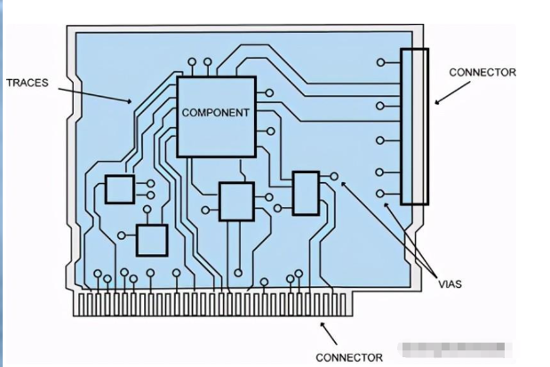
Figure 1: Printed Circuit Board
Multilayer boards often have a full layer of solid copper planes dedicated to distributing power to components on the board. These planes are often named after the component connections they connect. For example, a component that connects all V-shaped Cocos to power is often called a V-Cocos plane
The placement and routing of components often play a critical role in determining the electromagnetic compatibility of products that use printed circuit boards. Well-laid-out boards themselves do not generate significant radiation, and they do a good job of reducing currents and magnetic fields that might couple noise into cables or other objects outside the board. They are also configured to minimize the chances of external currents or magnetic fields coupling interfering signals into the board.
Printed Circuit Board Layout Strategies
Most board designers use a list of guidelines to help place components and route traces. For example, a typical guideline might be “Minimize the length of all traces carrying digital clock signals.” Often, designers are unfamiliar with the reasoning for the guideline or do not fully understand the consequences of violating it for a particular application.
Quiz Questions
Suppose you are laying out a high-speed multilayer printed circuit board, and you need to route a trace carrying a high-frequency signal from a digital component to an analog amplifier. You want to minimize the potential for electromagnetic compatibility (EMC) problems, so you search the web for EMC design guidelines and find three guidelines that seem relevant to your situation:
Reduce the length of high-speed traces as much as possible;
Allow gaps in any solid planes between analog and digital circuits;
Never route a high-speed trace across a gap in a signal return plane.
In Figure 2, you can draw a path directly between the two paths in the figure. The second routing strategy spaces the planes but routes the trace over the gap. The third routing strategy routes the trace around the gap. Each of these alternatives violates one of the guidelines. Which is the best choice?
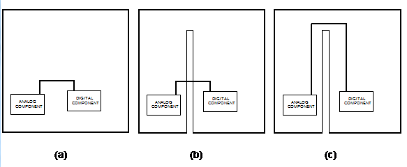
Figure 2: Which is the best trace routing choice?
Is each choice equally good because it meets 2 of the 3 guidelines? Are they all bad because they all violate at least one of the guidelines? These are questions that board designers face every day. Making the right choice can be the difference between a board that meets all the requirements and one that has serious radiated emissions or susceptibility issues. In this case, one of the choices is much better than the other two. Before we get to the right answer, however, let’s develop a strategy for evaluating printed circuit board layouts. With the right strategy, the correct answer to this quiz question should become obvious.
In this tutorial, we will explore 4 steps every EMC engineer should take when laying out a printed circuit board or looking at an existing board design. Those steps are:
Identify Potential EMI Sources and Victims
Determine Critical Current Paths
Identify Potential Antenna Components
Explore Possible Coupling Mechanisms
By taking the above steps first, component placement and trace routing decisions will become clearer. It should also be more obvious which design guidelines are most important for a particular design and which ones are not important at all.
Identify Potential EMI Sources and Victims
A typical circuit board may have dozens, hundreds, or even thousands of circuits. Each circuit is a potential source of energy that could end up being unintentionally coupled to other circuits or devices. Each circuit is also a potential victim of unintentionally coupled noise. However, some circuits are more likely to be noise sources than others, while others are more likely to be victims. EMC engineers (and board designers) should be able to identify which circuits are potential good sources and which ones are likely to be the most susceptible. Circuits of particular interest are discussed below.
Digital Clock Circuits
Synchronous digital circuits use a system clock that must be sent to every active component (on or off the board) that needs to interpret digital signals. Clock signals switch constantly and have narrowband harmonics. They are often among the most energetic signals on a printed circuit board. Therefore, it is not uncommon to see narrowband radiated emissions peaks at harmonics of the clock frequency, as shown in Figure 3.
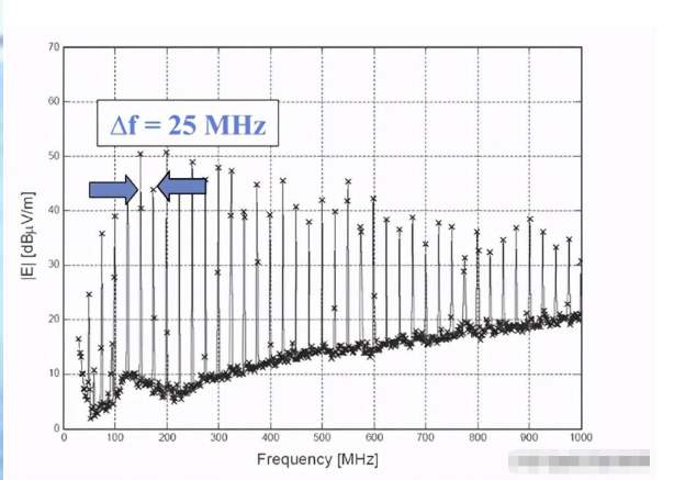
Figure 3: Radiated emissions from a 25MHz clocked product.
In this figure, the radiated emissions are clearly dominated by the harmonics of the 25MHz clock. The noise floor of 200–1000 MHz is the thermal noise of the spectrum analyzer used to make the measurement (corrected to reflect the antenna factor). In order for this product to meet FCC or CISPR Class B radiated emissions specifications, the clock source amplitude must be reduced, the inadvertent “antenna” efficiency must be reduced, or the source-antenna coupling path must be weakened.
Digital Signals
Most traces on a digital printed circuit board carry digital information, not clock signals. Digital signals are not periodic like clock signals, and their random nature results in a wider band of noise. Frequently switching digital signals can generate emissions similar to clock signals. An example is the least significant bit on a microprocessor address bus, since single-stepping through consecutive addresses causes this signal to toggle at the clock rate. The exact form and intensity of digital signal radiation depends on many factors, including the software running and the encoding scheme employed. In general, data signals are less troublesome than clock signals; however, high-speed data can still generate a significant amount of noise.
Power Switching Circuits
Switching power supplies and DC-DC converters generate different voltages by rapidly switching currents on and off through transformers. Typical switching frequencies are in the 10-100kHz range. This switching generates current spikes that can couple noise into the power output and other devices on the board. Although this noise signal is relatively periodic (i.e., narrowband harmonics), it appears as broadband noise during radiated emission noise testing because the distance between harmonic frequencies is below the resolution bandwidth of the measurement.
The noise floor peak near 120MHz in Figure 3 is caused by power switching noise. In this product, the switching noise is negligible relative to the clock noise. However, in other products, the power switching noise dominates because only the higher harmonics of the switching noise fall within the frequency range of the measured radiated emission noise. Power switching noise can be reduced by reducing the transition time of the switching circuit. However, this reduces the efficiency of the power supply, so alternative methods are preferred. Possible solutions are discussed in the Conducted EMI Tutorial.
Analog Signals
Analog signals can be broadband or narrowband, high frequency or low frequency. If your board uses analog signals, it is a good idea to be familiar with what these signals look like in the time and frequency domains. Narrowband, high frequency analog signals are particularly difficult to handle. Fortunately, because analog signals tend to be sensitive to low levels of noise, signal integrity considerations usually dictate that they be arranged in a way that will minimize radiated emissions.
DC Power Supplies and Slow-Speed Digital Signals
In general, DC power supplies and low-speed digital signals are troublesome if they do not have adequate power at the frequencies of radiated emissions. However, these traces are often the source of the most difficult radiated emissions problems. This is because the high-frequency voltages and currents inadvertently generated on these lines can be as large or larger than those on high-speed lines.
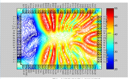
Figure 4: Near Magnetic Field Above a Packaged Integrated Circuit.
Figure 4 shows a plot of the near magnetic field above a dynamic random access memory module commonly used in personal computers. The near magnetic field provides an indication of the current flowing in the lead frame of the component package. The frequency measured is the third harmonic of the clock frequency. Note that more current is drawn from the DC power pins than from the signal pins.
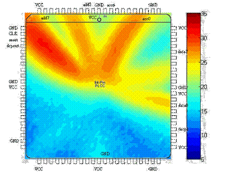
Figure 5: Near Magnetic Field Above a Microprocessor
Figure 5 shows a similar near magnetic field plot above a microprocessor implemented in a field programmable gate array (FPGA). In this plot, we see that the current injected into some of the low-speed address lines is almost as strong as the current in the clock signal.
How do high-frequency currents and voltages appear on low-frequency data lines? There are several ways this can happen. Most have to do with the design and layout of the integrated circuits (ICs) to which these lines are connected. Some ICs are very good at rejecting internally generated noise, while others are not. A poor design will produce high-frequency voltage fluctuations on every input and output trace connected to the IC. A good design can be relatively quiet.
When laying out a printed circuit board with an unfamiliar IC, it is best to treat every pin on that IC as a high-frequency source with the same characteristics as the internal clock. Otherwise, the power or slow-speed digital traces may be the most significant sources of radiation.
Identifying Current Paths
Perhaps the most important difference between digital circuit designers and EMC engineers is that EMC (and signal integrity) engineers pay close attention to the currents and voltages flowing in the circuit. This is a very important point. Most bad designs are caused by ignoring where the signal current may flow.
Although it has been discussed in previous sections, current path identification is so important to good printed circuit board design that it is necessary to review the main concepts here. First and foremost,
- Current flows in a loop.
Current flowing out of one side of the source must be drawn in on the other side. Also, - Current takes the path of least impedance.
At low (kHz and lower) frequencies, the impedance is dominated by the resistance, so the current takes the path of least resistance. At high (MHz and higher) frequencies, the impedance is dominated by the inductance term, so the current takes the path of least inductance.
Consider the board layout shown in Figure 6. A 50 MHz signal propagates from component A to component B on a trace above a plane. We know that, therefore, there must be an equal amount of current flowing from component B to component A. In this case, we assume that the current flows out of the pin of component B and returns to the pin of component A marked as GND. Since a solid plane is provided and the ground pins of both components are close together, it is easy to conclude that the current takes the shortest path between them. However, we now know that this is incorrect. High-frequency currents take the path of least inductance or the path of least loop area. Therefore, most of the signal current returning to the plane flows in the narrow path (path 2) directly under the signal trace.
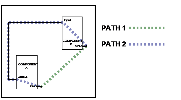
Figure 6: Which path does the signal return current take?
As shown in Figure 7, if the plane has a gap for any reason, a gap in position 2 will have little effect on signal integrity or radiated emissions. However, a gap in position 1 can cause significant problems. Current returning on the plane is forced to go around the gap under the trace. This greatly increases the signal loop area.
At low frequencies (typically kHz and below), the resistance of the plane tends to spread out the current so that current flowing between two distant points can cover a large portion of the board, as shown in Figure 8. On mixed-signal boards with low-frequency analog and digital components, this can be problematic. Figure 9 illustrates how a well-placed gap in the ground plane can protect circuits located in a specific area of the board from low-frequency return currents flowing within the plane.
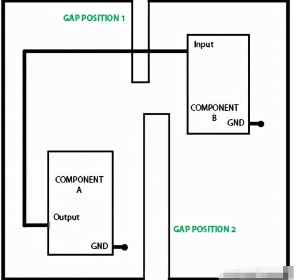
Figure 7: Which split location affects the flow of signal return current?
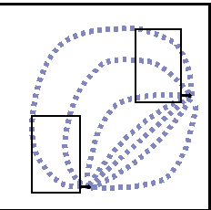
Figure 8: Low frequency return current path
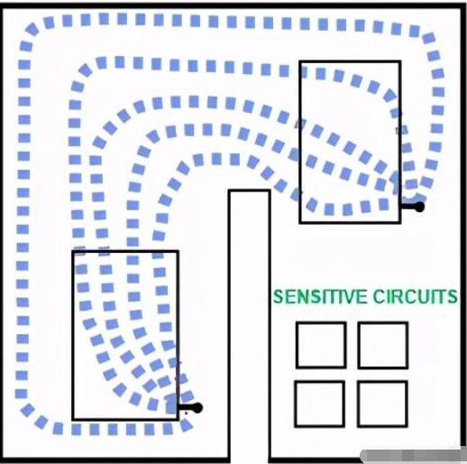
Figure 9: Low frequency return current path with split plane .
Identifying Antennas
The section on electromagnetic radiation points out that for most of the unexpected antennas that EMC engineers encounter to radiate effectively, essentially 3 conditions must be met:
The antenna must have two parts;
Neither part can be electrically small;
Something must induce a voltage between the two parts.
Most PCBs are electrically small at frequencies below 100MHz (LPs > 3m). This means that any effective antenna component must be relatively large compared to most board components. Typically, at low frequencies, the only viable antenna components are the attached cables and/or the metal chassis. If the PCB is laid out in a way that minimizes the possibility of inducing a voltage between any two of these possible antenna components, then it is less likely to have radiated **** or radiated susceptibility problems.
Figure 10 shows two PCB layouts. The connector and chassis connection represent possible efficient antenna components. Layout #2 is less likely to have radiated coupling problems below 100MHz because it is less likely to induce significant voltage between any two conductors that could act as an effective antenna. This can be achieved by simply placing both connectors on the same side of the board.
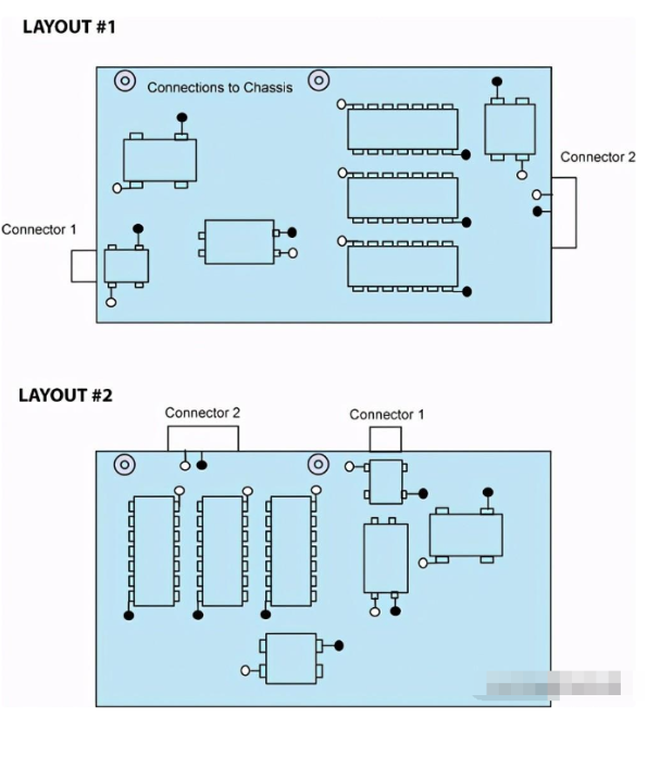
Figure 10. Two PCB layouts.
At frequencies above 100MHz, the wavelength is shorter and objects mounted on the board (or on the board itself) are more likely to be efficient antenna components. However, even at frequencies up to a few gigahertz, these antenna components should be relatively easy to spot. For example, at 1GHz, the wavelength in free space is 30cm. A quarter wavelength is 7.5cm.
Therefore, an effective antenna component must be at least a few centimeters long and driven relative to an object that is equally large or larger. Recall that differential currents (currents whose return path is nearby) are relatively inefficient sources of radiation. This means that a trace located next to or above its current return path is not a good antenna part. Therefore, if half of the antenna is a metal plane on the board, the other half must be raised, away from the plane. This helps make these antenna components easy to identify even at relatively high frequencies. Table 1 lists common antenna components on PCBs above and below 100MHz.
Table 1: PCB objects that may or may not be part of a good antenna.
Good antenna parts
Bad antenna parts
< 100 MHz
100MHz
< 100 MHz
100MHz
Cables
Heatsinks
Power planes
Microstrip or stripline traces
Microstrip or stripline traces
Tall components
Anything not too large
Seams in shielded enclosures
Identifying coupling mechanisms
Once we have identified a potential source or victim and a potential antenna, good PCB layout is about minimizing the coupling between the two. Earlier, we learned that there are only 4 categories of possible electromagnetic coupling mechanisms:
Conduction coupling
Electric field coupling
Magnetic field coupling
Radiation
Because we are talking about coupling between a source and an antenna on the same PCB, it is unlikely that we will have radiated coupling. Therefore, we only need to consider three coupling mechanisms. Conductive coupling will only occur if the source we have identified directly drives a good antenna component relative to another. An example of conductive coupling is when a signal trace is long enough to act as an effective antenna component driven relative to the signal return plane, but is not routed on that plane. In this case, the source would be the signal source and the antenna would be the trace plane pair. Radiate directly onto other conductors near the antenna to avoid radiating directly onto other conductors that are close to the source.
Conductive coupling is easy to spot once the source and antenna components are identified. However, field coupling mechanisms are often less obvious. To make field coupling more intuitive, it is convenient to think of electric field coupling as coupling proportional to the source voltage (voltage driven) and magnetic field coupling proportional to the source current (current driven).
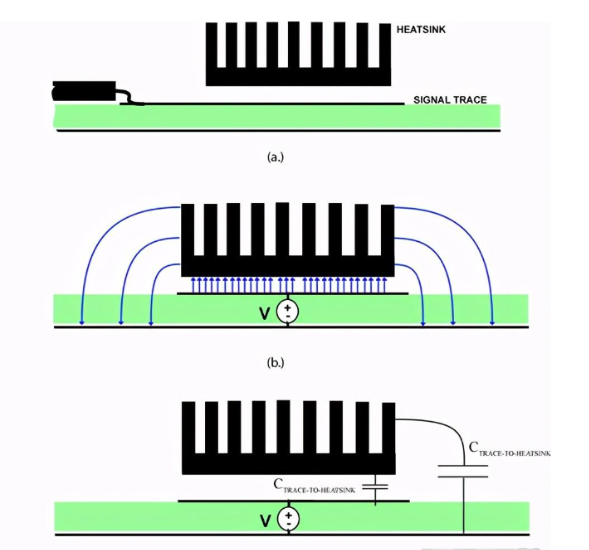
Figure 11: Printed circuit board trace coupled to heat sink.
Voltage driven coupling
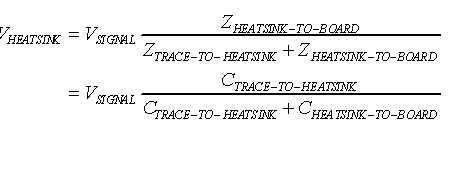
An example of voltage driven coupling leading to radiated heat is shown in Figure 11(a), which shows a signal trace routed under a heat sink. If the heat sink is not electrically small, it could be an effective antenna component. The metal planes of the circuit board are another potential antenna component. The trace is not directly connected to the heat sink, so there is no conductive coupling path. However, the voltage on the trace can drive the heat sink relative to the board because the electric field lines between the trace and the board are intercepted by the heat sink, as shown in Figure 11(b). This electric field coupling can be represented by capacitance, as shown in Figure 11(c). The voltage induced on the heat sink relative to the board is given by
Typically, board designers avoid routing high-speed signal traces directly under large heat sinks. Another more common example of voltage-driven coupling is shown in Figure 12. An active component is sandwiched between the printed circuit board and the heat sink. Again, neither the board nor the heat sink are electrically small at the frequencies of interest. As shown in Figure 12(a), the average voltage on the component is not equal to the voltage on the board because the component absorbs high-frequency currents through the finite connection inductance. This voltage drives the surface of the component relative to the board surface, as shown in the model in Figure 12(b). There is no direct connection between the heat sink and the power supply, so we cannot couple. However, the capacitance between the component surface and the heat sink provides an indirect (electric field) connection.
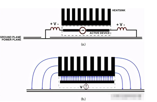
Figure 12: Component voltage driving heat sink relative to the board.
Note that in this example, it is the current driving the inductor that creates the source voltage. In other words, there is a magnetic field in the coupling process. However, the field coupling the component to the antenna is an electric field, and the radiated power is proportional to the voltage of the component relative to the board. Therefore, we still call it voltage-driven coupling.
Current-Driven Coupling
When the coupling between the source and the antenna is due to a magnetic field proportional to the signal current, it is called a current-driven coupling. Circuit designers usually think of signals as voltages, so it is unlikely that they will accidentally drive a good antenna with a signal voltage. However, if they ignore where the current flows, their design is likely to drive two good antenna components in a magnetic field.
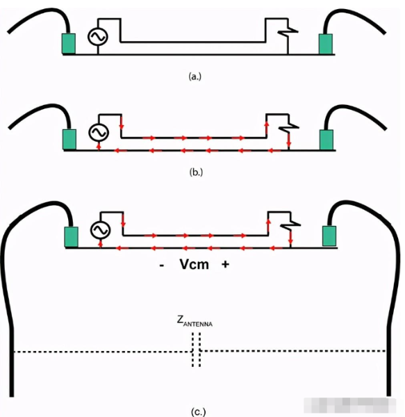
Figure 13 shows a very common example of current-driven coupling. A well-designed board has connectors on each side. We will now assume that the cable is fully shielded, with the cable shield connected to the “ground” plane on the board. A circuit consisting of a microstrip line driven at one end and terminated at the other end is located between the two connectors.
We have already seen that microstrip lines are not effective sources of radiated power, so the only possible antenna components in this design are the two cable shields, which are both “grounded”. We expect the two antenna components to be at the same potential since they are connected to each other by a wide copper plane. However, remember that an important requirement of a “ground” conductor is that it carry no intentional power or signal current.
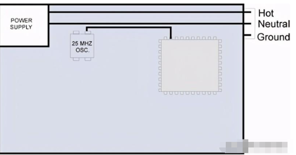
Figure 13: Example of current-driven coupling on a circuit board.
As shown in Figure 13(b), the “ground” plane in this design does carry signal current. In fact, current flowing in the plane generates a magnetic flux that surrounds the plane. If we consider the two cables as part of the antenna and represent the antenna current path by the antenna impedance, as shown in Figure 13(c), it is clear that the current flowing in the microstrip trace circuit will induce a voltage on the plane that drives one cable relative to the other.
Although the voltage induced on the plane is typically several orders of magnitude lower than the signal voltage, a few millivolts of noise on an efficient antenna is enough to exceed the radiated voltage requirements of the FCC and CISPR. In fact, it is difficult to meet radiated voltage requirements when high-speed digital components are located between connectors on an unshielded product board. On the other hand, when two connectors are adjacent, it is unlikely that the magnetic field will induce enough voltage between them to cause problems.
Direct Coupling to I/O
Although strictly speaking it is not a separate coupling mechanism, a common problem in PCB layout is coupling a noise source directly to a trace that can carry the noise off the board. An example is shown in Figure 14. A moderately high speed trace is routed together with another trace that connects to a connector. Voltage and/or current (via electric or magnetic fields) coupled from one trace to the other can propagate along the I/O trace and leave the board. In the example shown in the figure, the two antenna components can be either an I/O cable driven relative to the board or a wire in an I/O cable driven relative to another board.
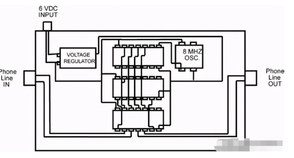
Figure 14: Possible coupling problem.
You might think this is a rare problem because it is fairly obvious once you see it. However, on a board with hundreds or thousands of traces, this situation often occurs. If the autorouter cannot check I/O traces routed near high speed traces, this should be done manually. The same applies to I/O traces routed near traces connected to vulnerable inputs, as the easiest way for radiated noise to enter the board is through the I/O.
Printed Circuit Board Design Guidelines
As mentioned earlier, many board designers use a series of guidelines to help place components and route traces. Now that we know more about noise sources, antennas, and coupling mechanisms on printed circuit boards, we can take a closer look at these design guidelines and understand their importance and significance. Listed below are 16 EMC design guidelines for printed circuit boards with a brief description of each guideline.
- The length of traces carrying high-speed digital signals or clocks should be minimized.
High-speed digital signals and clocks are often the strongest noise sources. The longer these traces are, the more opportunities there are for energy to be routed away from these traces. Also remember that loop area is often more important than trace length. Make sure there is a good high-frequency current return path near each trace.
- The length of traces that connect directly to connectors (I/O traces) should be minimized.
Traces that connect directly to connectors can be paths for energy to couple on or off the board.
- Signals with high-frequency content should not be routed underneath components used for board I/O.
Traces routed under a component can capacitively or inductively couple energy to that component.
- All connectors should be located on one edge or corner of the board.
Connectors are the most effective antenna components in most designs. Placing them on the same edge of the board makes it easier to control the common-mode voltage that can drive one connector relative to the other.
- No high-speed circuits should be located between input/output connectors.
Even if two connectors are located on the same edge of the board, high-speed circuits located between them can induce enough common-mode voltage to drive one connector relative to the other, resulting in significant radiation****.
- Critical signal or clock traces should be buried between power/ground planes.
Routing traces on a layer between two solid planes can well contain the fields of these traces and prevent unwanted coupling.
- Select active digital components with maximum acceptable off-chip transition times.
If the transition times of digital waveforms are faster than necessary, the power in higher-order harmonics can be much higher than necessary. If the transition times of the logic used are faster than necessary, series resistors or ferrites can often be used to slow them down.
- All off-board communications from a single device should be routed through the same connector.
Many components (especially large VLSI devices) generate a lot of common-mode noise between different I/O pins. If one of these devices is connected to more than one connector, this common-mode noise can drive a good antenna (the device is also more susceptible to antenna radiated noise.)
- High-speed (or sensitive) traces should be routed at least 2X from the edge of the board, where X is the distance between the trace and its return current path.
The electric and magnetic field lines associated with traces very close to the edge of the board are less complete. Crosstalk and coupling to antennas tend to be greater than with these traces.
- Differential signal traces should be routed together and at the same distance from any solid planes.
If differential signals are balanced (i.e. they are the same length and maintain the same impedance as other conductors), they are less susceptible to noise and less likely to radiate****.
- All power (e.g. voltage) planes that reference the same power return (e.g. ground) plane should be routed on the same layer.
For example, if a board uses 3.3V, 3.3V analog, and 1.0V; then it is generally desirable to minimize high frequency coupling between these planes. Placing the voltage planes on the same layer will ensure that there is no overlap. This will also help promote an efficient layout since it is unlikely that active devices will require two different voltages at any one location on the board.
- Spacing between any two power planes on a given layer should be at least 3 mm.
If two planes are too close together on the same layer, significant high frequency coupling can occur. Arcing or shorting can also be a problem under adverse conditions if the planes are spaced too closely.
- On boards with power and ground planes, no traces should be used to connect power or ground. Connections should be made using vias close to the component power or ground pads.
Traces connecting to a plane on another layer take up space and add inductance to the connection. If high frequency impedance is a concern (as with power bus decoupling connections), this inductance can significantly degrade the performance of the connection.
- If the design has more than one ground plane layer, any ground connection at a given location should be connected to all ground planes at that location.
The general guideline here is that high-frequency currents will take the most favorable (lowest inductance) path if allowed to. Do not try to direct the flow of these currents by connecting only to specific planes.
- There should be no gaps or seams in the ground plane.
It is usually best to have a solid ground (signal return) plane and a layer dedicated to that plane. Any additional power or signal current loops that must be DC-isolated from the ground plane should be routed on a layer other than the layer dedicated to the ground plane.
- All power or ground conductors on the board that are in contact with (or coupled to) the chassis, cables, or other good “antenna parts” should be connected together at high frequencies.
Unexpected voltages between different conductors (nominally called “grounds”) are a major source of radiated voltage and susceptibility problems.
In addition to the above 16 guidelines, board designers usually adopt guidelines specific to their industry. For example, “Clock generation circuitry employing a phase-locked loop should have its own separate power supply derived from the board’s power supply via a #1234 ferrite bead.” These experience-based guidelines are invaluable to the knowledgeable board designer. However, applying these same guidelines to other designs without knowing where they came from or why they work is a waste of effort and a non-functional board. It is very important to understand the underlying physics behind each guideline being applied.
It is also important to identify potential noise sources, antennas, and coupling paths with every design you evaluate. The best design will not be the one that meets the most guidelines. The best design is the one that meets all specifications at the lowest cost and with the highest reliability.
Putting it all together
So we have a list of design guidelines and a basic understanding of their importance and significance. Let’s try to apply them to the test question posed earlier, which asks which board layout in Figure 2 is best.
Hopefully, you can quickly eliminate option (b), the design with a trace crossing over the gap in the return plane. Option (a) employs the shortest trace and is therefore the best option, provided that the gap in the ground plane is truly unnecessary. If there is a low frequency common impedance coupling problem that makes the gap unavoidable, then option (c) is almost as good as option (a) in terms of routing this trace. Remember that the length of a microstrip signal trace is not as important as its total loop area.
Example 1: A Simple Single-Layer Board Layout
Harvey has invented a device that records phone calls made from his phone. The design is relatively simple, as shown in Figure 15. However, when it is connected to the phone line, the radiation from the device interferes with his television reception.
Redesign Harvey’s board to reduce radiated EMI. You can move components and/or add components, but you must use a single-sided board.
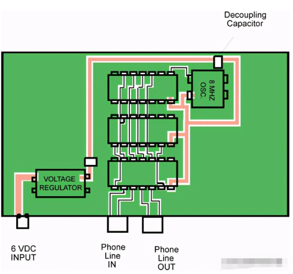
Figure 15: Harvey’s Circuit
We should start by identifying potential sources and antennas. Of course, the 8MHz clock signal is a potential source, as are the data lines. This device may also generate significant noise on the power trace. Potential antenna components are the three connectors. Nothing else on this board is large enough to be an effective radiator.
As we begin to rearrange components, we should try to place all antenna components (i.e., connectors) on one side of the board. We should also reorient the components to minimize the length of the traces. Finally, we should fill the empty areas on the board with ground and ensure that each signal trace has a nearby return path.
One solution to this problem is shown in Figure 16. Try tracing the path of the 8 MHz signal current in the Figure 15 layout compared to the same path in Figure 16. This current flows from the clock output pin of the oscillator, into the clock input pin of the upper IC, out the ground pin of the upper IC, and into the ground pin of the oscillator. This loop area is much smaller in the Figure 16 layout. Also note that there is no high frequency current return on the plane section between any two connectors in the Figure 16 layout.
The design in Figure 15 is unlikely to meet radiated emissions specifications and therefore cannot be sold. The design in Figure 16 should meet radiated emissions specifications in almost all countries without any shielding or high cost components. Note that we can provide vias for filtering components installed on the telephone line if we feel it is necessary.