Andiwn Circuits
PCB manufacturing and PCB Assembly
100% Quality Guarantee or Money back
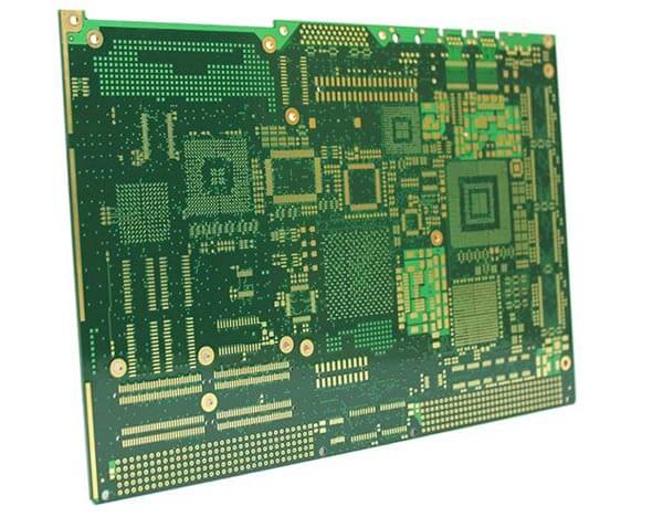
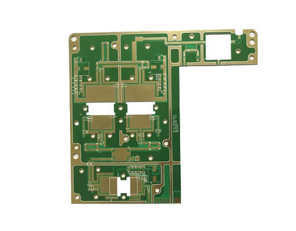
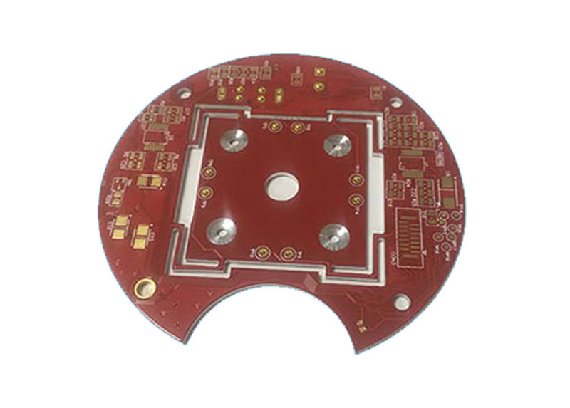
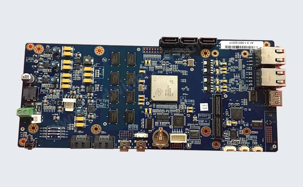
PCB Manufacturing
Andwin Circuits as a industry leading of PCB manufacturer since 2003.
Our multilayer PCB quick-turn service could support your product get-to-market faster,
100% quality guarantee that reduce the developer’s time and save money!
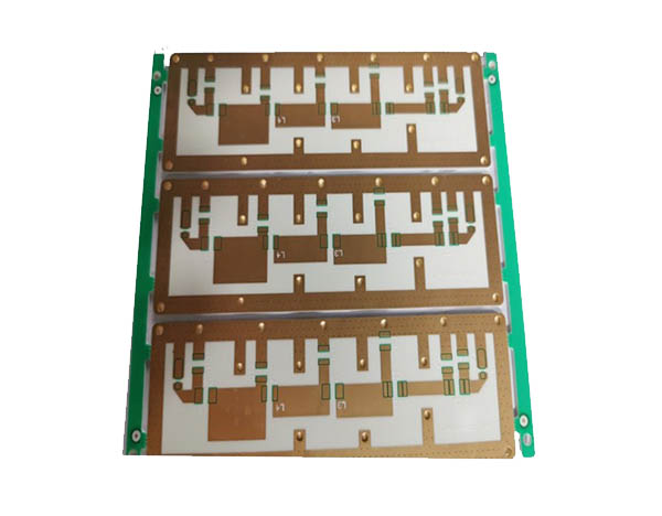
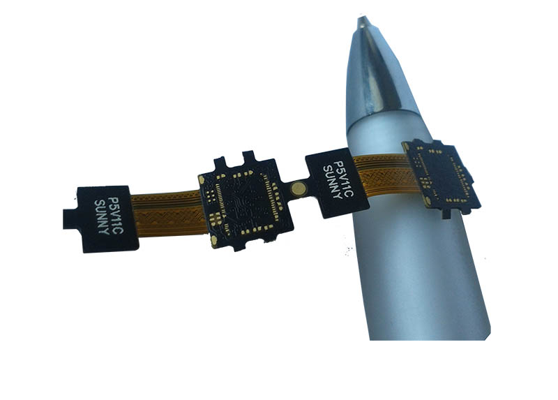
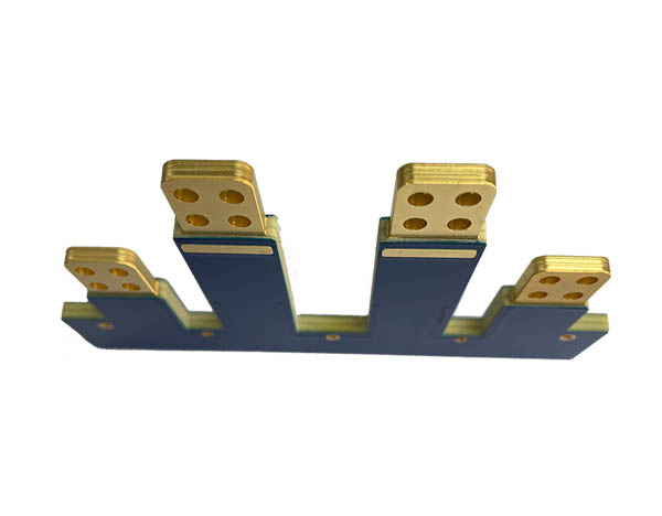
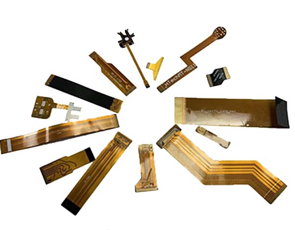
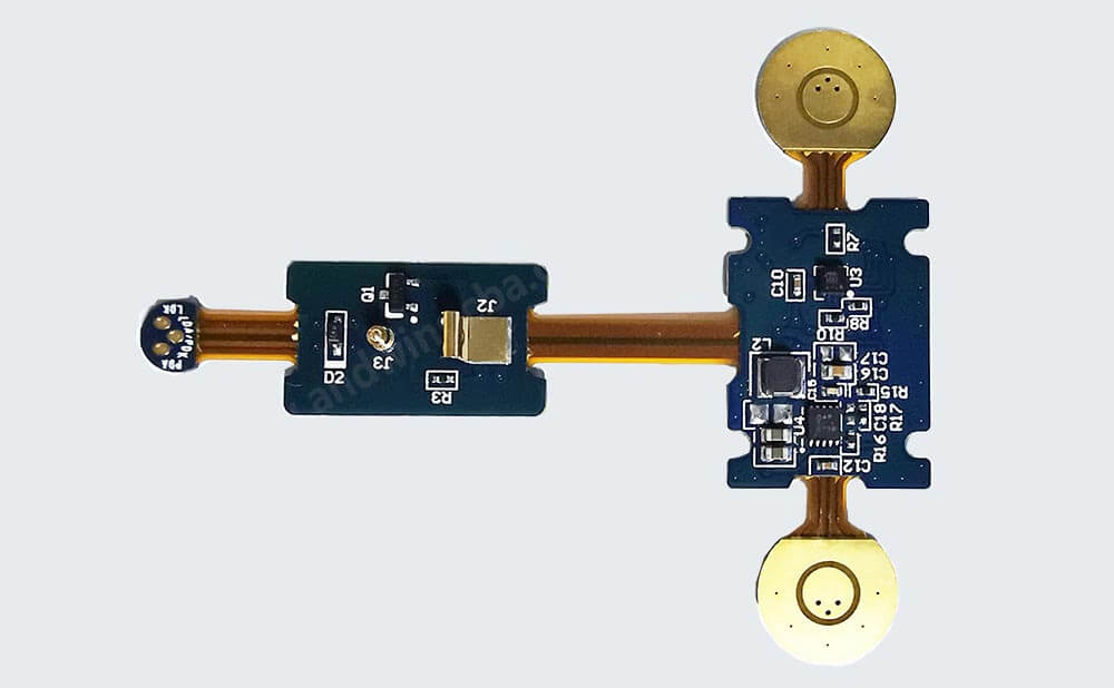
Rigid Flex PCB
6L HDI Rigid Flex PCB
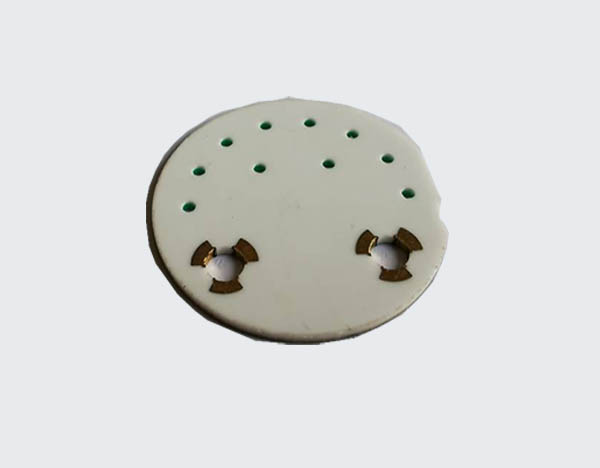
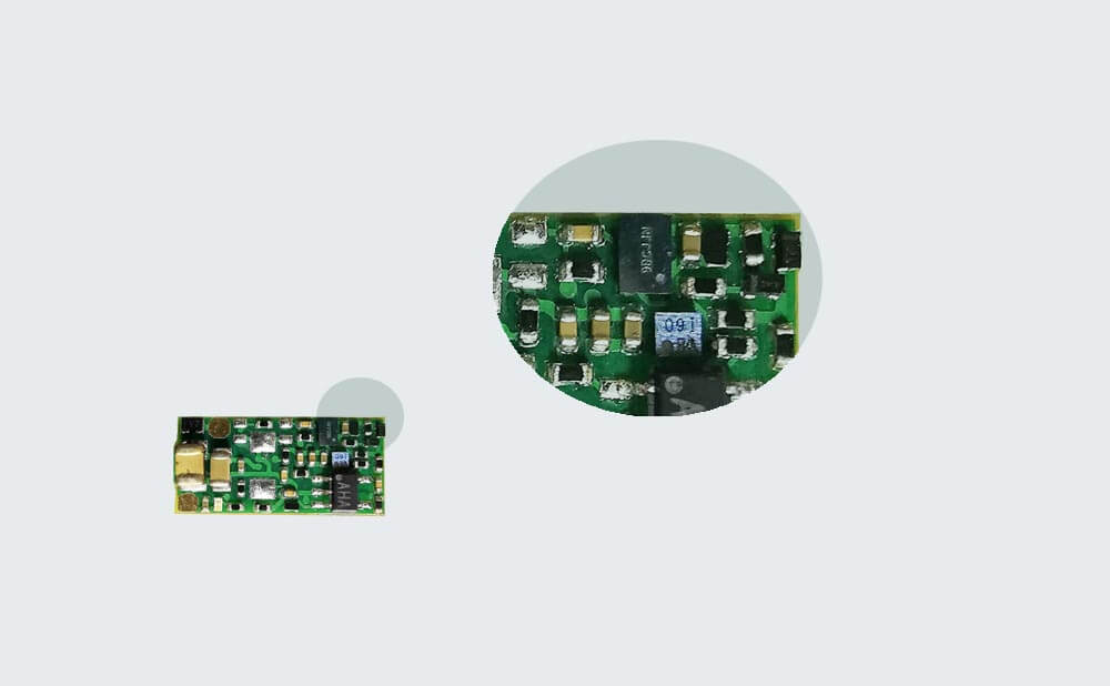
Metal Core PCB
2L Aluminum MCPCB
Turnkey PCB Assembly service
Turnkey Printed Circuit boards,components source and PCB assembly,
You throw the file to us, just waiting the PCBA arrived, saved time and economical more.key PCB Assembly service
100% Quality Guarantee or Money back
Turnkey PCB assembly
Quick turn PCB assembly
Low volume PCB assembly
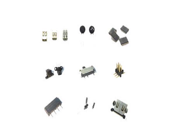
Components source
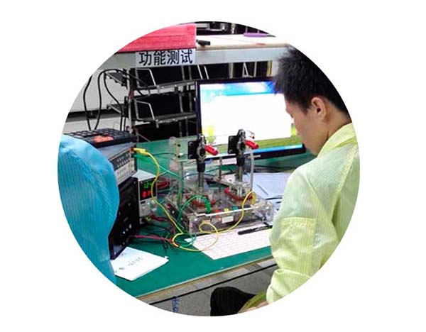
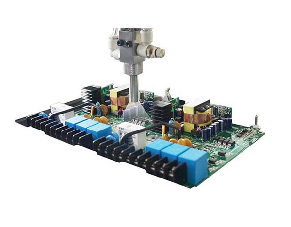
IC program and Testing
Conformal coating PCBA

Why Choose us?
- Response fast ( always in 3 Hours)
- More than 20+ Years in PCB Industry
- Engineers are 15+ Years PCB experience
- 100% DRC(Design rule Checking)
- 100% AOI (Automatic Optic Inspection)
- 100% Electronic Test( E-Test)
- 100% Quality guarantee,or money back
- Use the best raw material
Get professional one stop PCB solution from us!