PCB Board Assembly: A Comprehensive Guide
Introduction
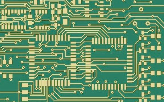
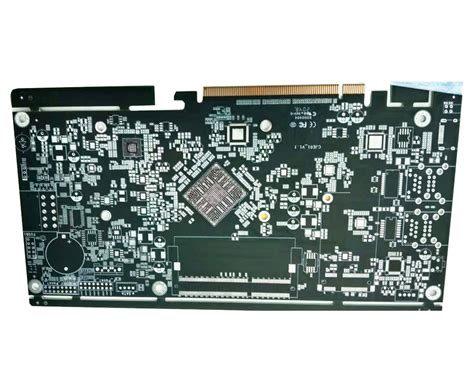
Printed circuit boards (PCBs) are the core components of modern electronic devices. Almost all electronic products rely on PCBs for electrical connections and signal transmission. The assembly process of PCBs is to install electronic components on PCBs to form a complete circuit. This article will explore various aspects of PCB assembly in depth, including its importance, process, technology, common problems and future development trends.
1.Importance of PCB Assembly
PCB assembly is a key link in the electronics manufacturing industry, which directly affects the performance, reliability and cost of products. High-quality PCB assembly can ensure the stable operation of electronic equipment, reduce the failure rate and improve the market competitiveness of products. In addition, with the trend of electronic products towards miniaturization and high performance, the technical requirements of PCB assembly are also constantly improving.
2. Basic Process of PCB Assembly
The basic process of PCB assembly usually includes the following steps:
(1)Design and Layout
In the initial stage of PCB assembly, engineers need to use electronic design automation (EDA) software for circuit design and layout. Factors such as component arrangement, signal integrity, and thermal management need to be considered during the design process. After the design is completed, the generated Gerber file will be used for subsequent PCB manufacturing.
(2)PCB manufacturing
PCB manufacturing is the process of converting the design into an actual circuit board. The process includes the following steps:
Material preparation: Select the appropriate substrate (such as FR-4) and copper foil.
Graphic transfer: Transfer the circuit pattern to the PCB through photolithography.
Etching: Remove excess copper to form a circuit.
Drilling: Drill holes according to design requirements to facilitate component installation and electrical connection.
Surface treatment: Treat the surface of the PCB to improve welding performance.
(3)Component placement
Component placement is the core step of PCB assembly, and there are two main methods:
Manual placement: Suitable for small-batch production or prototyping, simple operation, but low efficiency.
Automatic placement: Use a surface mount machine (SMT) for automatic component placement, suitable for large-scale production, high efficiency and high precision.
4.Soldering
Soldering is an important step in connecting components to PCBs. There are mainly the following welding methods:
Wave soldering: Suitable for plug-in components, the solder liquid is poured over the PCB through a wave soldering machine to achieve welding.
Reflow soldering: Applicable to surface mount components, solder paste is applied on the PCB, and then heated to melt the solder paste and connect with the components.
5.Testing and inspection
After assembly, the PCB needs to undergo rigorous testing and inspection to ensure the normal operation of the circuit. Common testing methods include:
Visual inspection: Visually inspect the appearance and welding quality of the PCB.
Functional test: Test the electrical performance of the PCB to ensure that it meets the design requirements.
Aging test: Test the reliability of the PCB through high temperature and high humidity environments.
6.Packaging and delivery
The PCBs that have passed the test will be packaged to ensure that they are not damaged during transportation. The packaging materials need to have anti-static and moisture-proof properties to protect the integrity of the PCB.
7 Key technologies in PCB assembly
With the advancement of science and technology, PCB assembly technology is also developing. Here are some key technologies:
(1)Surface mount technology (SMT)
SMT is the most commonly used technology in modern PCB assembly. It has the advantages of high density, miniaturization, and high degree of automation. The application of SMT has greatly improved the assembly efficiency of PCBs and reduced production costs.
(2)Automated equipment
The introduction of automated equipment makes the PCB assembly process more efficient and precise. The use of automated equipment such as automatic placement machines, reflow soldering machines, and testing equipment can reduce manual operations and improve production efficiency and product quality.
3.3D printing technology
The application of 3D printing technology in PCB assembly is gradually increasing, and it can achieve rapid manufacturing of complex structures. Through 3D printing, engineers can quickly make prototypes, conduct design verification, and shorten product development cycles.
4.Common problems in PCB assembly
During the PCB assembly process, some common problems may be encountered. The following are several typical problems and their solutions:
(1)Poor welding
Poor welding is one of the most common problems in PCB assembly, which may cause circuit failure or short circuit. Solutions include:
Ensure the control of welding temperature and time.
Use appropriate welding materials and solder paste.
Maintain welding equipment regularly to ensure its normal operation.
(2)Component damage
During the mounting and welding process, components may be damaged. To avoid such problems, it is recommended to:
Check the specifications and quality of components before mounting.
Ensure that electrostatic protection measures are in place during the mounting process.
(3)Failed test
Failed test may be caused by design defects or assembly problems. Solutions include:
Perform full simulation and verification in the design stage.
Perform comprehensive functional testing after assembly to find and solve problems in time.
5. Future development trends
With the continuous advancement of science and technology, the PCB assembly industry is also developing. Here are some future development trends:
(1)Smart manufacturing
Smart manufacturing will become the main trend of PCB assembly. Through technologies such as the Internet of Things (IoT), big data analysis and artificial intelligence (AI), the production process will be intelligent and automated, and production efficiency and product quality will be improved.
(2)Environmental protection and sustainable development
With the increase of environmental awareness, the PCB assembly industry is also transforming to green manufacturing. Using environmentally friendly materials, reducing waste emissions, and improving resource utilization will become important directions for the development of the industry.
(3)Multifunctional integration
Future PCBs will develop in the direction of multifunctional integration, integrating more functional modules such as sensors, wireless communications, etc. to meet the increasingly complex needs of electronic products.
Conclusion
PCB assembly is an indispensable part of the electronics manufacturing industry, and its importance is self-evident. With the continuous advancement of technology, the process and technology of PCB assembly are also evolving. Understanding the basic process, key technologies and common problems of PCB assembly will help improve the quality and reliability of products. In the future, the PCB assembly industry will develop in the direction of intelligence, environmental protection and multifunctional integration, providing stronger support for the innovation of electronic products.