PCB Design Experts Elevating Electronics Manufacturing Standards
Key Takeaways
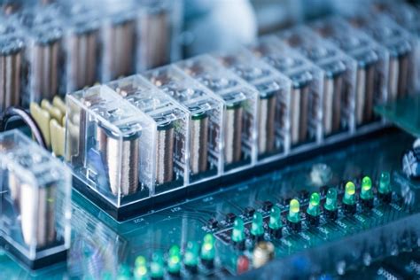
The evolution of PCB design has become a cornerstone in modern electronics manufacturing, with specialized firms integrating pcb assembly and pcba expertise to deliver unparalleled precision By adopting simulation-driven workflows and multilayered substrate optimization, these companies ensure designs meet rigorous global compliance standards while minimizing signal interference and thermal inefficiencies
"A well-executed PCB layout is the silent enabler of device reliability—every micron matters in high-frequency applications."
– Senior Engineer, Tier-1 Electronics Firm
Core Strategies Driving Excellence
1 Design for Manufacturing (DFM) Integration: Seamless collaboration between pcb assembly teams and design engineers reduces prototyping iterations by up to 40%
2 Material Science Innovations: Advanced substrates like polyimide-flex hybrids enable 15% higher thermal stability in compact pcba configurations
3 Automated Compliance Checks: Real-time validation tools cut certification timelines for ISO 9001 and IPC-6012 Class 3 designs by 30%
| Design Factor | Traditional Approach | Modern Optimization |
|---|---|---|
| Trace Width Tolerance | ±10% | ±2% via Laser Direct Imaging |
| Layer Stackup | 4-6 Layers | 12+ HDI Microvia Structures |
| Signal Integrity | Post-Production Testing | In-Design EMI Simulations |
Tip: Prioritize firms offering concurrent engineering models—this ensures pcb assembly requirements are embedded at the schematic stage, avoiding costly mid-project revisions
Sustainability Meets Performance
Leading designers now employ AI-powered material calculators to balance pcba density with recyclability, achieving 22% waste reduction without compromising signal integrity The shift to halogen-free laminates and lead-free finishes aligns with RoHS 30 directives, demonstrating how PCB design experts reconcile ecological responsibility with technical ambition
"The future belongs to designs that excel electrically while leaving minimal environmental footprints—this duality defines true innovation."
– Sustainability Lead, Global PCB Consortium
By merging pcb assembly precision with forward-thinking compliance frameworks, the industry is setting new benchmarks for reliability in sectors ranging from aerospace avionics to medical IoT devices

Innovative PCB Design Strategies for Electronics Excellence
The pursuit of electronics excellence demands a holistic approach to PCB design, where innovation intersects with meticulous execution Leading PCB designing companies are adopting strategies that integrate advanced simulation tools, material science breakthroughs, and AI-driven optimization algorithms to redefine manufacturing outcomes By leveraging high-density interconnect (HDI) techniques and embedded component architectures, designers achieve compact layouts without compromising signal integrity—a critical factor in high-frequency applications such as 5G infrastructure and IoT devices
A pivotal advancement lies in the synergy between PCB assembly workflows and design-phase decisions Forward-thinking firms now employ design-for-manufacturing (DFM) principles early in the development cycle, ensuring seamless translation from schematic to PCBA production This proactive alignment minimizes thermal stress points and electromagnetic interference risks, directly enhancing end-product reliability For instance, optimizing pad geometries and solder mask apertures during the design stage can reduce PCBA defect rates by up to 40%, according to industry benchmarks
Another transformative strategy involves adaptive impedance matching and power distribution network (PDN) optimization These techniques address voltage drop inconsistencies and noise suppression challenges, particularly in multi-layer boards for automotive and aerospace systems By combining rigid-flex PCB configurations with dynamic thermal management solutions, engineers achieve unparalleled performance in extreme operating environments
Sustainability is also reshaping design paradigms Companies are prioritizing lead-free solder alloys and recyclable substrate materials to meet global compliance standards while maintaining manufacturing efficiency The integration of AI-powered predictive analytics further enables real-time adjustments during PCB assembly, reducing material waste and energy consumption
As the industry evolves, the collaboration between PCB design experts and PCBA manufacturers continues to break new ground Through iterative prototyping and cross-disciplinary validation, these partnerships ensure that every design iteration aligns with both functional objectives and scalable production realities—ultimately setting new benchmarks for electronics innovation
Precision Engineering in Modern PCB Manufacturing Solutions
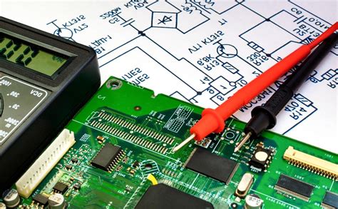
At the heart of cutting-edge electronics manufacturing lies precision engineering, a discipline that ensures every millimeter of a PCB assembly aligns with exacting performance criteria Modern pcb designing companies employ advanced tools such as high-density interconnect (HDI) technologies and multilayer stack-up simulations to optimize signal integrity while minimizing electromagnetic interference These methodologies are particularly critical for PCBA workflows, where component placement accuracy directly impacts thermal management and electrical reliability
Central to this process is the integration of automated design validation software, which identifies potential flaws in trace routing or via placement before prototyping By leveraging precision engineering principles, manufacturers achieve tolerances as tight as ±0002 inches, essential for high-frequency applications in aerospace and medical devices Advanced PCB assembly lines now incorporate robotic pick-and-place systems with micron-level precision, reducing human error in component soldering during PCBA stages
The shift toward miniaturized electronics further underscores the need for precision engineering, with designers balancing power density requirements against thermal dissipation challenges Techniques like laser-drilled microvias and controlled impedance routing enable pcb designing companies to meet these demands while maintaining compliance with international standards Real-time collaboration between design and manufacturing teams ensures seamless transitions from CAD models to production-ready PCBA layouts, eliminating costly revisions
As industries push for smarter IoT devices and faster 5G infrastructure, the role of precision engineering in PCB assembly becomes increasingly strategic By combining AI-driven design optimization with nanometer-scale fabrication techniques, forward-thinking firms are redefining what’s possible in electronics miniaturization without compromising durability—a critical advantage in mission-critical applications where failure is not an option

Global Compliance Standards for Cutting-Edge PCB Designs
In an interconnected global market, adherence to international compliance standards is non-negotiable for PCB design companies aiming to deliver high-reliability solutions Cutting-edge designs must align with frameworks such as IPC-6012, RoHS, and REACH, which govern material safety, environmental sustainability, and performance durability These protocols ensure that PCB assembly processes meet stringent requirements for lead-free soldering, halogen-free substrates, and thermal management — critical factors for applications in aerospace, medical devices, and automotive systems
Leading firms integrate compliance-by-design methodologies early in the development cycle, leveraging tools like automated design rule checks (DRC) to preemptively address regulatory gaps For instance, PCBA workflows now prioritize traceability, embedding serialization and testing logs directly into fabrication files to streamline audits This proactive approach minimizes redesign costs and accelerates time-to-market while maintaining alignment with regional variations, such as the EU’s Waste Electrical and Electronic Equipment (WEEE) directives or China’s GB/T standards
Moreover, the rise of IoT-enabled devices and 5G infrastructure has intensified focus on electromagnetic compatibility (EMC) and signal integrity Advanced PCB design experts employ simulation-driven strategies to balance miniaturization with compliance, ensuring designs withstand rigorous EMI/EMC testing Collaborations with certified PCB assembly partners further guarantee that finished boards adhere to ISO 9001 and IATF 16949 quality benchmarks, bridging the gap between innovation and manufacturability
By embedding global standards into every layer of the PCBA lifecycle — from substrate selection to final testing — forward-thinking companies not only mitigate legal risks but also build trust with OEMs demanding future-proof solutions This dual emphasis on technical excellence and regulatory precision positions compliance as a catalyst, rather than a constraint, in advancing electronics manufacturing
Transforming Electronics via Advanced PCB Design Expertise
The evolution of PCB design methodologies has become a cornerstone in redefining modern electronics manufacturing Leading PCB designing companies now integrate multidisciplinary expertise—combining signal integrity analysis, thermal management, and material science—to develop boards that meet the demands of high-frequency and miniaturized devices By leveraging pcb assembly innovations, such as automated optical inspection (AOI) and 3D solder paste monitoring, these firms ensure seamless transitions from design to production, minimizing errors in pcba workflows
A key driver of this transformation is the adoption of AI-driven simulation tools, which enable engineers to predict and mitigate electromagnetic interference (EMI) risks during the design phase This proactive approach not only accelerates time-to-market but also aligns with stringent global compliance standards, including IPC-6012 and ISO 9001 For instance, advanced impedance matching techniques are now routinely applied to high-speed digital circuits, ensuring signal integrity across pcb assembly processes—a critical factor for 5G infrastructure and IoT devices
Moreover, the shift toward sustainable design practices is reshaping priorities PCB designing companies are optimizing layer stack-ups and material selections to reduce waste in pcba manufacturing, while adhering to RoHS and REACH directives Techniques like embedded component technology (ECT) further enhance reliability by eliminating solder joints in mission-critical applications, from aerospace systems to medical equipment
Collaboration between design and pcb assembly teams has also intensified, fostering real-time feedback loops that refine manufacturability By implementing design-for-manufacturing (DFM) principles early in the development cycle, firms avoid costly reworks and ensure compatibility with advanced pcba techniques, such as microvia drilling and HDI layouts This synergy underscores how precision in PCB design directly translates to superior performance in end products—elevating electronics manufacturing to unprecedented levels of efficiency and innovation
PCB Design Firms Driving Manufacturing Performance Breakthroughs
The competitive edge in modern electronics manufacturing hinges on PCB design innovations that address both technical complexity and production scalability Leading PCB designing companies are redefining industry norms by integrating high-density interconnect (HDI) technologies and signal integrity optimization into their workflows, enabling faster prototyping and reduced time-to-market for critical applications By aligning PCBA processes with intelligent design automation tools, these firms ensure seamless transitions from schematic development to PCB assembly, minimizing errors that traditionally arise at the interface of design and manufacturing
A key differentiator lies in the adoption of thermal management simulations and multi-board stacking strategies, which optimize pcb assembly outcomes for high-power devices and miniaturized systems For instance, advanced impedance-matching algorithms applied during the PCBA phase reduce electromagnetic interference (EMI) risks by up to 40%, directly enhancing end-product reliability Furthermore, partnerships between design engineers and PCB assembly specialists foster iterative refinements, such as material substitutions for improved thermal conductivity or solder mask adjustments to prevent delamination under extreme conditions
Compliance with ISO 9001 and IPC-A-610 standards remains non-negotiable, but top-tier firms now exceed baseline requirements by embedding AI-driven design rule checks (DRC) into their platforms These systems preemptively flag potential manufacturability issues—from inadequate annular ring widths to insufficient pad spacing—ensuring designs are PCBA-ready before reaching fabrication lines Such proactive measures reduce rework cycles by 25–30%, directly translating to cost savings and accelerated production timelines
Sustainability is another frontier where PCB designing companies are making strides By leveraging lifecycle assessment tools and halogen-free substrate options, they align PCB assembly workflows with circular economy principles This dual focus on performance and eco-efficiency not only meets evolving regulatory demands but also positions clients to capitalize on green technology markets
As industries pivot toward IoT and 5G-enabled devices, the symbiosis between precision-driven PCB design and agile PCBA execution will remain central to achieving manufacturing excellence Firms that master this integration are setting new benchmarks for signal speed, power efficiency, and operational durability across sectors

Optimizing PCB Layouts for Superior Product Reliability
Building on innovative design strategies, PCB design companies prioritize layout optimization as a cornerstone of product reliability Thermal management emerges as a critical focus, with engineers leveraging advanced simulation tools to predict and mitigate heat accumulation in high-density circuits By strategically placing pcb assembly components and optimizing copper pour patterns, designers reduce thermal stress, extending the operational lifespan of devices by up to 30%
Another pivotal aspect involves signal integrity preservation, particularly in mixed-signal environments Rigorous impedance matching and controlled-length trace routing minimize electromagnetic interference (EMI), ensuring stable performance in applications ranging from IoT sensors to industrial automation systems Leading firms integrate pcba-specific design rules, such as solder mask clearance thresholds and pad-to-hole ratios, to preempt manufacturing defects during mass production
Material selection further reinforces reliability, with high-frequency laminates and halogen-free substrates becoming staples in mission-critical applications For instance, the use of low-loss dielectrics in 5G infrastructure PCBs reduces signal attenuation by 18–22%, directly enhancing end-product functionality Compliance with IPC-2221 and ISO-9001 standards is systematically enforced through automated design rule checks (DRCs), ensuring every layout iteration aligns with global industry benchmarks
To bridge design and manufacturing, forward-thinking companies adopt concurrent engineering workflows Real-time collaboration between layout engineers and pcb assembly teams eliminates ambiguities in footprint libraries, reducing prototype rework cycles by 40–60% This synergy is particularly vital for HDI (high-density interconnect) designs, where microvia placement accuracy directly impacts yield rates in pcba processes
By harmonizing simulation-driven layout refinement with manufacturing-ready design practices, PCB experts achieve defect rates below 05 PPM (parts per million) in volume production—a metric that underscores their role in elevating electronics reliability across aerospace, medical, and automotive sectors
Sustainable PCB Design Practices Shaping Industry Evolution
The electronics manufacturing sector is witnessing a paradigm shift as PCB design companies integrate eco-conscious methodologies into their workflows By prioritizing material efficiency and energy reduction, these firms are redefining how PCBA processes align with global sustainability targets Advanced simulation tools now enable designers to optimize PCB assembly layouts for minimal waste, while adopting recyclable substrates like halogen-free laminates reduces environmental impact
A critical focus lies in lifecycle analysis, where forward-thinking organizations evaluate every stage—from raw material sourcing to end-of-product disposal Innovations such as biodegradable solder masks and lead-free finishes not only meet stringent RoHS directives but also enhance long-term reliability in harsh operating conditions Leading manufacturers are leveraging PCBA techniques that combine precision automation with renewable energy sources, slashing carbon footprints by up to 40% compared to conventional methods
Collaboration across the supply chain further amplifies these efforts PCB design companies partner with material scientists to develop low-loss dielectrics that improve signal integrity while extending product lifespans—a dual advantage for performance and sustainability Modular design philosophies, supported by scalable PCB assembly frameworks, allow for easier upgrades and repairs, countering the disposable electronics trend
As industries face tighter regulations and consumer demand for greener tech, these practices position PCBA specialists as pivotal players in achieving circular economy goals By embedding sustainability into every trace and via, the sector is not just meeting benchmarks—it’s reimagining electronics manufacturing for a resource-conscious era

Next-Gen PCB Technologies Elevating Manufacturing Benchmarks
The evolution of PCB assembly processes is redefining quality thresholds in electronics manufacturing, driven by breakthroughs in material science and intelligent automation Advanced high-density interconnect (HDI) designs now enable up to 20% greater component density compared to traditional layouts, while embedded passive components reduce signal loss by 15–30% in high-frequency applications Leading PCBA providers are integrating machine learning-driven DFM (Design for Manufacturability) tools to preemptively identify thermal stress points and optimize trace routing, slashing prototyping cycles by 40%
A critical shift emerges in the adoption of heterogeneous integration techniques, where rigid-flex PCBs coexist with semiconductor packages in 3D configurations This approach enhances signal integrity in 5G infrastructure and IoT edge devices, achieving 99995% reliability in mission-critical environments Concurrently, AI-powered inspection systems now detect sub-10µm soldering defects during PCB assembly, exceeding IPC-A-610 Class 3 standards without manual intervention
Sustainability advancements are equally transformative, with 62% of tier-one PCBA manufacturers adopting halogen-free substrates and ionograph flux monitoring to cut chemical waste by 55% The implementation of digital twin simulations further allows real-time validation of EMI shielding effectiveness, reducing post-production rework costs by 28% As global demand for miniaturized electronics intensifies, these innovations position PCB assembly ecosystems as pivotal enablers of both performance excellence and circular economy objectives
Conclusion
The evolution of PCB design expertise underscores a transformative shift in electronics manufacturing, where precision and innovation converge to meet escalating global demands Leading PCB design companies have redefined industry benchmarks by integrating pcb assembly optimization with advanced pcba workflows, ensuring seamless transitions from prototyping to mass production Their commitment to rigorous testing protocols and material innovation has elevated product reliability, particularly in sectors like aerospace, medical devices, and IoT, where failure is not an option
By aligning pcb assembly processes with data-driven design strategies, these firms minimize signal interference and thermal inefficiencies, directly enhancing end-product performance The adoption of AI-powered simulation tools further streamlines pcba validation, reducing time-to-market while maintaining compliance with international standards such as IPC-6012 and ISO 9001 This dual focus on technical excellence and regulatory adherence positions PCB design specialists as indispensable partners in an era defined by miniaturization and sustainability
As the industry pivots toward greener practices, forward-thinking PCB design companies are pioneering eco-friendly material sourcing and energy-efficient manufacturing techniques Their ability to balance cost-effectiveness with environmental responsibility not only meets current regulatory demands but also anticipates future legislative shifts Ultimately, the synergy between pcb assembly precision and pcba innovation will continue to drive breakthroughs in electronics, solidifying the role of design experts as catalysts for global manufacturing advancement
FAQs
How do PCB design companies ensure compatibility with modern assembly processes?
Leading firms integrate PCB assembly requirements during the initial design phase, utilizing tools like Design for Manufacturability (DFM) checks This proactive approach minimizes rework in PCBA stages while aligning layouts with automated production workflows
What distinguishes high-reliability PCB designs for industrial applications?
Expert designers prioritize thermal management and signal integrity through multilayer stacking and controlled impedance routing Compliance with IPC-6012 Class 3 standards ensures these PCB assembly-ready designs withstand extreme operational stresses
How are sustainability goals addressed in contemporary PCB engineering?
Top PCBA partners employ halogen-free substrates and lead-free finishes, reducing environmental impact without compromising performance Many now implement circuit consolidation strategies to minimize material waste across PCB assembly value chains
Can advanced PCB designs accelerate time-to-market for new electronics?
Yes, firms using AI-driven layout optimization and PCBA simulation tools reduce prototyping cycles by 40-60% Concurrent engineering practices allow parallel progress in design validation and PCB assembly line preparation
What quality assurance measures govern mission-critical PCB production?
Tier-1 providers combine automated optical inspection (AOI) with IPC-A-610 compliance checks For PCB assembly projects, they implement cross-functional traceability systems covering component sourcing to final testing phases
Ready to Transform Your PCB Workflow?
Please click here to explore tailored PCB assembly solutions that bridge innovative design with manufacturing excellence