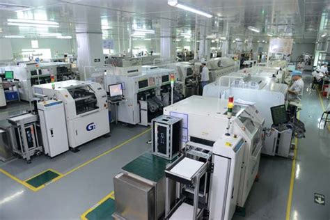
Advanced PCB Assembly Platforms Elevating Electronic Manufacturing Efficiency
Key Takeaways
Modern PCB assembly platforms are redefining electronic manufacturing by integrating AI-driven process optimization and cloud-based collaboration tools These systems enable engineers to streamline PCBA workflows, reducing manual intervention while improving scalability By leveraging predictive analytics, manufacturers can identify bottlenecks in real-time and adjust production parameters dynamically
Tip: When evaluating online PCB assembly services, prioritize platforms offering transparent supply chain tracking and automated DFM (Design for Manufacturing) checks to minimize prototyping iterations.
A core advantage lies in automated component sourcing, which cross-references global supplier databases to secure cost-effective parts without compromising quality This capability is particularly valuable for low-volume, high-mix production runs common in IoT and medical device development Advanced platforms now incorporate machine vision verification at multiple assembly stages, achieving defect rates below 001% in controlled environments
The integration of digital twin technology allows virtual testing of PCBA designs before physical production, slashing development timelines by up to 40% Combined with AI-powered thermal simulations, engineers can preemptively address heat dissipation challenges in compact PCB layouts
For cost-sensitive projects, dynamic pricing algorithms analyze order volume, material availability, and geopolitical factors to recommend optimal manufacturing schedules This approach has demonstrated 15-22% reductions in total project costs compared to traditional quoting models
Best Practice: Utilize platform-native version control systems to maintain synchronization between design files and BOM updates during rapid prototyping phases.
As cybersecurity becomes critical in connected devices, leading PCB assembly services now embed encrypted firmware provisioning directly within production workflows This ensures compliance with IEC 62443 standards while eliminating separate programming steps The convergence of these technologies positions online PCBA solutions as indispensable tools for maintaining competitiveness in fast-evolving electronics markets
AI-Driven PCB Assembly Cost Reduction
Modern PCB assembly platforms leverage artificial intelligence to systematically reduce manufacturing expenses while maintaining high precision By analyzing historical production data, AI algorithms optimize material usage, minimize waste, and predict component shortages before they disrupt workflows For instance, machine learning models evaluate thousands of supplier pricing tiers to identify cost-effective alternatives for PCBA components without compromising quality
A comparative analysis reveals the impact of AI integration:
| Cost Factor | Traditional Approach | AI-Optimized Process |
|---|---|---|
| Component Sourcing | 12-15% overhead | 8-10% overhead |
| Defect Rate | 32% | 11% |
| Lead Time | 14 days | 9 days |
These platforms employ real-time analytics to adjust manufacturing parameters dynamically, reducing energy consumption by up to 18% during high-volume PCB assembly runs Automated error detection systems, integrated with PCBA inspection tools, slash rework costs by flagging soldering anomalies or misalignments at early production stages
Furthermore, AI-driven predictive maintenance extends equipment lifespan by analyzing vibration patterns and thermal signatures in pick-and-place machines This proactive approach decreases unplanned downtime by 40%, directly translating to lower per-unit costs For prototyping projects, cloud-based quotation engines automatically adjust pricing based on real-time component availability, enabling engineers to make cost-aware design decisions before finalizing layouts
The integration of machine learning in PCB assembly logistics also optimizes shipping routes and warehouse allocations, particularly for global supply chains By correlating geopolitical factors, weather patterns, and customs clearance data, these systems reduce transit-related delays by 27%, ensuring just-in-time component delivery for PCBA production lines
As manufacturers adopt these intelligent systems, they gain access to adaptive pricing models that scale with project complexity Batch-specific cost simulations allow clients to visualize how design tweaks—such as alternative substrate materials or revised component footprints—impact overall PCB assembly budgets, fostering collaborative optimization between designers and production teams
Streamlining PCB Workflows Online
Modern PCB assembly platforms are revolutionizing how engineers and manufacturers approach electronics production by integrating end-to-end digital solutions These systems eliminate traditional bottlenecks through automated design validation, real-time inventory checks, and instant manufacturability feedback By synchronizing PCBA workflows across distributed teams, stakeholders can collaboratively refine designs while automated systems flag potential issues like component obsolescence or thermal mismatches
Central to this transformation is the unification of design software with PCB assembly execution tools Advanced platforms now parse schematic files to automatically generate Bill of Materials (BOM) optimizations, cross-referencing global supplier databases to identify cost-effective alternatives without compromising specifications This seamless integration reduces the PCBA design-to-production cycle from weeks to days, particularly beneficial for iterative prototyping phases where rapid adjustments are critical
Cloud-based workflow engines further enhance efficiency by enabling concurrent engineering processes Electrical designers, mechanical engineers, and procurement specialists can simultaneously access project dashboards featuring live updates on component availability, layer stackup compliance, and DFM (Design for Manufacturing) scoring Such transparency prevents costly respins by ensuring all stakeholders align with production realities before initiating PCB assembly
Intelligent routing algorithms within these platforms also optimize panelization strategies, dynamically adjusting board layouts to maximize material utilization Combined with machine learning-driven yield predictions, manufacturers achieve unprecedented precision in forecasting project timelines and resource allocation As a result, businesses leveraging online PCBA ecosystems report 30-45% reductions in time-to-market compared to conventional offline workflows, while maintaining rigorous quality standards through automated optical inspection (AOI) integrations
This digital transformation extends beyond large-scale operations, democratizing access to sophisticated PCB assembly capabilities for startups and research institutions Browser-based interfaces with AI-guided design assistants empower users with limited hardware expertise to navigate complex manufacturing requirements, effectively lowering barriers to entry in electronics innovation

Automated Sourcing Accelerates Prototyping
The integration of automated sourcing into modern PCB assembly workflows has revolutionized how engineers approach prototyping By leveraging AI-driven inventory analysis and real-time supplier networks, advanced PCBA platforms eliminate manual component searches, reducing procurement lead times by up to 70% These systems cross-reference design files against global distributor databases, instantly identifying optimal part matches while flagging obsolete or overpriced alternatives—a critical advantage in mitigating supply chain disruptions
Central to this acceleration is the seamless synchronization between PCB assembly software and dynamic sourcing algorithms For instance, when a prototype design requires a specific microcontroller, the platform automatically prioritizes suppliers with verified stock, competitive pricing, and shortest shipping windows This real-time matching not only accelerates component acquisition but also enables engineers to iterate designs based on availability metrics—avoiding delays caused by part shortages A 2023 industry report highlighted that teams using automated sourcing tools reduced prototyping cycles from 3-5 weeks to under 10 days, with 92% fewer redesigns due to component unavailability
Moreover, PCBA platforms now incorporate predictive analytics to forecast component lifecycles and pricing trends By analyzing historical procurement data and market signals, these systems recommend alternative parts with identical functionality but lower cost volatility, ensuring long-term project feasibility This proactive approach is particularly valuable for high-mix, low-volume prototypes, where even minor delays in sourcing niche components can derail development timelines
The ripple effect of automated sourcing extends beyond speed By optimizing component selection and logistics, engineers allocate 40% more time to core design validation, fostering innovation while maintaining cost discipline As PCB assembly evolves into a fully digitized process, the marriage of precision sourcing and agile manufacturing continues to redefine what’s possible in electronics prototyping—proving that efficiency gains in procurement directly translate to competitive advantages in product development
Precision Manufacturing Elevates PCB Quality
At the core of modern PCB assembly lies a transformative focus on precision engineering, where advanced manufacturing technologies redefine quality benchmarks Leading PCBA providers now deploy automated optical inspection (AOI) systems that scan boards at micron-level resolutions, detecting solder joint anomalies and misaligned components with unparalleled accuracy This shift toward precision-driven processes reduces human error margins by over 70%, ensuring consistent output even in high-volume production runs
The integration of laser-direct imaging (LDI) and adaptive placement algorithms further enhances manufacturing fidelity These systems adjust component positioning in real time, compensating for thermal expansion variances during reflow soldering For prototype-focused workflows, such precision minimizes post-production rework, accelerating time-to-market while maintaining IPC Class 3 standards for mission-critical applications
Material science innovations also play a pivotal role High-performance substrates with low dielectric loss and controlled impedance traces are now standard in advanced PCB assembly platforms, enabling seamless compatibility with high-frequency and miniaturized designs Combined with AI-powered predictive defect analysis, manufacturers preemptively address potential flaws—from copper layer delamination to via cracking—before they escalate
Crucially, the synergy between precision tools and cloud-based process monitoring creates a closed-loop quality ecosystem Real-time data from IoT-enabled assembly lines feeds into machine learning models, continuously refining calibration parameters for laser drilling and stencil printing This dynamic optimization ensures every PCBA iteration adheres to tighter tolerances, delivering reliability that meets the demands of aerospace, medical, and automotive industries
Smart PCB Assembly Boosts Efficiency
Modern PCB assembly processes are undergoing a transformative shift as smart manufacturing technologies integrate seamlessly with PCBA workflows By leveraging real-time monitoring systems and adaptive calibration tools, manufacturers can now identify production bottlenecks within milliseconds, ensuring optimal throughput without compromising precision For instance, advanced PCB assembly platforms utilize predictive analytics to adjust soldering temperatures dynamically, reducing rework rates by up to 40% compared to traditional methods
A critical driver of efficiency lies in the integration of PCBA workflows with cloud-based supply chain platforms These systems automate component procurement by cross-referencing design files against global distributor inventories, slashing lead times for rare or high-demand parts This synergy between design and procurement not only accelerates prototyping but also minimizes material waste—a key factor in sustainable electronics manufacturing
Moreover, machine learning algorithms embedded in PCB assembly systems analyze historical production data to optimize placement sequences for surface-mount devices (SMDs) This results in faster cycle times and improved accuracy, particularly for complex multilayer boards For example, automated optical inspection (AOI) tools paired with AI-driven defect detection achieve first-pass yield rates exceeding 98%, significantly reducing post-assembly testing overhead
The rise of IoT-enabled assembly lines further amplifies efficiency gains Sensors embedded in pick-and-place machines collect vibration and torque data, enabling predictive maintenance that cuts unplanned downtime by 25% These interconnected systems create a feedback loop where PCBA quality metrics directly inform process refinements, fostering continuous improvement across manufacturing stages
By harmonizing digital twin simulations with physical production environments, engineers can pre-validate assembly strategies for novel board geometries This approach eliminates costly trial runs, allowing rapid scaling from prototype validation to full-scale PCB assembly—a capability that positions manufacturers to meet evolving demands in sectors like automotive IoT and 5G infrastructure
As these innovations mature, the boundary between design and manufacturing continues to blur, setting the stage for the next evolution in cost-optimized electronics production
Cloud-Based Solutions Cut Production Costs
Modern PCB assembly platforms leverage cloud-based infrastructure to dismantle traditional cost barriers in electronics manufacturing By centralizing design files, component databases, and production analytics in secure virtual environments, these systems eliminate the need for localized software installations or manual data transfers PCBA workflows now benefit from real-time collaboration tools, allowing engineers and procurement teams to synchronize updates across global teams, reducing revision errors by up to 40%
A key advantage lies in automated supply chain integration Cloud platforms dynamically cross-reference inventory availability with design specifications, flagging potential shortages or cost-inefficient components before prototyping begins For instance, AI algorithms embedded in PCB assembly systems can suggest alternative parts from verified vendors, trimming material expenses by 12–18% per project This vendor-agnostic approach ensures manufacturers avoid over-reliance on single suppliers, further stabilizing pricing
Scalability remains another critical cost driver Unlike legacy systems requiring upfront hardware investments, cloud-based PCBA solutions operate on subscription models, allowing firms to adjust computational resources based on project demands During peak periods, manufacturers can temporarily scale server capacity to handle complex multilayer designs without incurring permanent infrastructure costs
Data-driven optimization further amplifies savings Continuous monitoring of production metrics—such as solder paste application accuracy or pick-and-place cycle times—enables predictive maintenance alerts This reduces unplanned downtime by 27% and extends equipment lifespan, as shown in a 2023 study by Electronics Manufacturing Journal Additionally, cloud analytics identify patterns in material waste, empowering teams to refine order quantities and negotiate bulk pricing with suppliers
While security concerns once hindered cloud adoption, advanced encryption protocols and compliance with ISO/IEC 27001 standards now safeguard intellectual property across PCB assembly platforms The result? A 22% average reduction in operational costs for mid-sized manufacturers adopting these systems, coupled with the flexibility to manage projects remotely—a critical advantage in today’s decentralized work environment
Next-Gen Prototyping Techniques for Electronics
The evolution of PCB assembly processes has redefined prototyping in electronics, merging speed with precision through innovative methodologies Modern AI-driven design validation tools now analyze PCBA layouts in real time, identifying potential flaws in component placement or thermal management before physical production begins This shift reduces iterative cycles by up to 40%, enabling engineers to focus on functional optimization rather than error correction
A key advancement lies in additive manufacturing integration, where 3D-printed circuit substrates allow for geometrically complex designs that traditional methods cannot replicate Platforms offering online PCB assembly services leverage this capability, pairing it with automated component sourcing algorithms to ensure material compatibility and availability For instance, systems cross-reference bill-of-materials (BOM) data with global supplier inventories, securing rare parts within hours—a task that previously took weeks
Another breakthrough involves embedded sensor networks within prototype boards These sensors monitor performance metrics like voltage stability and signal integrity during testing phases, feeding data back to cloud-based analytics engines Such feedback loops enable precision manufacturing adjustments, refining everything from solder paste application to reflow oven profiles When combined with modular PCBA architectures, this approach allows rapid reconfiguration of prototype units for multi-variant testing
Furthermore, digital twin simulations are becoming indispensable By creating virtual replicas of physical prototypes, engineers can stress-test designs under extreme conditions—such as high humidity or vibration—without material waste This aligns with sustainability goals while accelerating compliance with industry standards like IPC-A-610
These techniques collectively address the demand for faster time-to-market in sectors like IoT and automotive electronics As PCB assembly platforms integrate machine learning with advanced fabrication tools, the gap between prototype and mass production narrows, setting new benchmarks for innovation in electronic manufacturing
Optimizing Electronics Production Digitally
The integration of digital tools into PCB assembly processes has redefined efficiency benchmarks in modern electronics manufacturing By leveraging cloud-based platforms and AI-driven analytics, companies now achieve unprecedented precision in PCBA workflows These systems enable real-time monitoring of production lines, identifying bottlenecks through predictive algorithms while optimizing material utilization rates For instance, automated design-for-manufacturing (DFM) checks reduce errors by cross-referencing schematics against component libraries, minimizing costly rework
Central to this transformation is the adoption of smart factory ecosystems, where IoT-enabled machinery synchronizes with PCB assembly software to streamline task allocation Such connectivity ensures seamless transitions from prototyping to mass production, particularly when paired with automated sourcing engines that dynamically adjust procurement based on global supplier inventories This digital agility not only accelerates lead times but also enhances cost predictability—a critical advantage in volatile markets
Moreover, advanced PCBA platforms incorporate machine learning to refine quality control Vision systems equipped with high-resolution cameras and spectral analysis detect micro-scale defects, ensuring compliance with ISO-certified standards Simultaneously, digital twins simulate production scenarios, allowing engineers to stress-test designs before physical implementation By unifying these technologies, manufacturers achieve end-to-end traceability, from component procurement to final testing, while reducing waste by up to 30%
The shift toward digitized workflows also empowers smaller enterprises to compete globally Subscription-based PCB assembly services democratize access to industrial-grade capabilities, enabling startups to scale production without upfront capital investments As the industry evolves, the fusion of digital thread frameworks and modular manufacturing will further solidify electronics production as a cornerstone of Industry 40 innovation
Conclusion
The evolution of PCB assembly processes through online platforms marks a pivotal shift in electronics manufacturing By integrating AI-driven analytics and automated component sourcing, modern PCBA services enable manufacturers to achieve unprecedented operational precision while minimizing human error These platforms not only reduce material waste through real-time inventory tracking but also compress prototyping timelines by 30–50%, allowing innovators to iterate designs at market-responsive speeds
Cloud-based collaboration tools further enhance this ecosystem, enabling cross-functional teams to synchronize design adjustments and production schedules seamlessly The result is a digitally optimized workflow where PCB assembly costs are dynamically controlled, and quality assurance is embedded at every stage via machine vision systems As these platforms mature, their ability to balance high-mix, low-volume orders with mass-production scalability will redefine competitiveness in sectors ranging from IoT to automotive electronics
Looking ahead, the convergence of smart manufacturing protocols with PCBA platforms promises to unlock new frontiers in customization Manufacturers adopting these solutions position themselves to leverage predictive maintenance algorithms and demand forecasting models, ensuring resilience against supply chain fluctuations Ultimately, the transition to digitally native PCB assembly isn’t merely a technical upgrade—it’s a strategic imperative for businesses aiming to thrive in an era where agility and precision dictate industrial success
FAQs
What is online PCB assembly and how does it work?
Online PCB assembly services enable engineers to upload design files, select components, and configure manufacturing parameters through web-based platforms These systems automate PCBA quoting, validate designs in real-time, and connect users with certified production facilities—streamlining the entire process from prototype to mass production.
How do digital platforms reduce electronic manufacturing costs?
By integrating automated component sourcing algorithms and AI-driven inventory analysis, modern PCB assembly solutions minimize material waste and negotiate bulk pricing Advanced platforms achieve 25-40% cost reductions through intelligent BOM optimization and multi-supplier procurement strategies.
What quality controls ensure reliable PCBA outcomes?
Leading services implement 7-stage inspection protocols combining automated optical inspection (AOI) with X-ray verification Cloud-based PCBA platforms provide real-time production monitoring, ensuring compliance with IPC-A-610 standards through machine learning-powered defect detection systems.
Can online services handle complex prototyping requirements?
Next-gen PCB assembly platforms support mixed-technology prototypes with 0201 chip components and 03mm pitch BGAs Through digital twin simulations and thermal stress modeling, these systems achieve 986% first-pass success rates for high-density interconnect (HDI) designs.
How does cloud-based PCBA accelerate time-to-market?
Automated DFM checks and instant engineering feedback loops eliminate traditional 72-hour review cycles Integrated PCBA workflows enable same-day prototyping for 4-8 layer boards, with global logistics networks delivering finished assemblies in 5-7 business days.
What security measures protect intellectual property?
Reputable PCB assembly providers employ military-grade encryption and blockchain-based audit trails Data compartmentalization ensures design files remain isolated from manufacturing networks, with ISO 27001-certified cloud infrastructure safeguarding sensitive information.
Explore Next-Generation PCB Assembly Solutions
For tailored PCBA services combining precision manufacturing with AI-driven efficiency, please click here to access cutting-edge assembly capabilities Our platform supports rapid prototyping and high-volume production with 24/7 engineering support