AOI PCB Assembly: A Key Technology to Improve Electronic Manufacturing Quality
Introduction
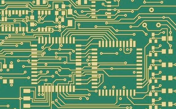
In modern electronic manufacturing, printed circuit boards (PCBs) are the core components of electronic devices. With the continuous advancement of technology, the design and production of PCBs have become increasingly complex. In order to ensure the quality and reliability of products, automated optical inspection (AOI) technology plays a vital role in the PCB assembly process. This article will explore the principles, processes, advantages and future development trends of AOI PCB assembly.
1.What is AOI?
Automated Optical Inspection (AOI) is a method of inspecting PCBs using optical imaging technology. It captures images of the PCB surface with a high-resolution camera and compares them with pre-set standards to identify potential defects. These defects may include missing components, component misalignment, solder joint defects, short circuits and open circuits.
2.The Importance of AOI in PCB Assembly
2.1 Improve Production Efficiency
AOI technology can perform real-time inspections at all stages of PCB assembly, detect problems in a timely manner, and reduce the time and cost of manual inspections. Through automated inspections, the efficiency of the production line can be significantly improved.
2.2 Improve product quality
AOI systems can detect tiny defects on PCBs with high precision, ensuring that each PCB meets quality standards. This high-precision detection capability greatly reduces the defective rate of products and improves the reliability of the overall product.
2.3 Reduce rework costs
By detecting defects at an early stage, AOI can effectively reduce the cost of rework and repair in the later stage. Timely defect detection can avoid sending problematic products to subsequent assembly and testing stages, saving time and resources.

3.Workflow of AOI PCB assembly
3.1 Design stage
Before the implementation of the AOI system, the design and layout of the PCB must be carried out first. Designers will use professional PCB design software to create circuit diagrams and layout diagrams and generate corresponding design files.
3.2 Manufacturing stage
During the manufacturing process of PCBs, the AOI system will perform inspections at multiple key nodes:
Solder paste printing inspection: After the solder paste is printed, the AOI system will check the thickness, position and shape of the solder paste to ensure that the quality of the solder paste meets the standards.
Component placement inspection: After the component placement is completed, the AOI system will detect the accuracy of the component, including the type, position and orientation of the component to ensure that it meets the design requirements.
Post-welding inspection: After welding is completed, the AOI system will inspect the solder joints to identify the quality, shape and defects of the solder joints.
3.3 Data analysis and feedback
The AOI system will record the inspection results in the database and generate detailed reports. This data can be used to analyze problems in the production process and help engineers optimize the design and production process.
4.Advantages of AOI technology
4.1 High-precision inspection
The AOI system is equipped with high-resolution cameras and advanced image processing algorithms to detect tiny defects. This high-precision inspection capability makes AOI an indispensable tool in the PCB assembly process.
4.2 Real-time inspection
The AOI system can perform real-time inspections during the production process, detect problems in a timely manner and provide feedback. This real-time performance greatly improves production efficiency and reduces the generation of defective products.
4.3 Flexibility
Modern AOI systems are highly flexible and can adapt to PCBs of different types and sizes. This enables manufacturers to quickly switch between multiple products to meet changes in market demand.
4.4 Cost-effectiveness
Although the initial investment in AOI systems is relatively high, AOI technology can bring significant cost benefits to companies in the long run by improving production efficiency, reducing defect rates and reducing rework costs.
5.Challenges of AOI Technology
Although AOI technology has many advantages, it still faces some challenges in practical applications:
5.1 Complex PCB design
With the continuous development of electronic products, the design of PCBs has become more and more complex, which may cause difficulties for AOI systems when detecting. Complex layouts and small-sized components may affect the accuracy of detection.
5.2 Data processing
The amount of data generated by AOI systems is huge, and how to effectively process and analyze this data is a challenge. Manufacturers need to invest in data analysis tools and technologies to make full use of the data provided by AOI systems.
5.3 Technology updates
With the rapid development of technology, AOI systems also need to be continuously updated and upgraded to maintain their competitiveness. Manufacturers need to regularly invest in equipment maintenance and upgrades.
6.Future Development Trends of AOI Technology
6.1 Artificial Intelligence and Machine Learning
In the future, artificial intelligence (AI) and machine learning technologies will be widely used in AOI systems. This will enable AOI systems to identify defects more intelligently and improve the accuracy and efficiency of detection.
6.2 3D AOI Technology
Traditional AOI mainly relies on 2D images for detection, while 3D AOI technology can provide more comprehensive detection capabilities. 3D AOI can better identify the height and shape of solder joints, further improving the accuracy of detection.
6.3 Integrated Solutions
Future AOI systems will pay more attention to integration with other production equipment to achieve full automation of production lines. This will further improve production efficiency and reduce the possibility of human error.
6.4 Data-driven decision-making
With the development of big data technology, AOI systems will be able to provide more in-depth data analysis to help manufacturers make more accurate decisions. This will promote the continuous optimization of the production process.
Conclusion
Automatic optical inspection (AOI) technology plays an indispensable role in PCB assembly. By improving the accuracy and efficiency of inspection, AOI not only improves product quality, but also reduces production costs. Despite some challenges, the future development of AOI technology is still promising. With the continuous advancement of artificial intelligence, 3D technology and data analysis, AOI will continue to play an important role in the electronics manufacturing industry and bring greater competitive advantages to enterprises.