s Leading PCB Assembly Companies for Advanced Solutions
Key Takeaways
When evaluating PCB assembly providers, several critical factors emerge as industry benchmarks Leading global manufacturers distinguish themselves through advanced PCBA capabilities that integrate surface-mount technology (SMT) with high-density interconnect (HDI) designs, particularly for mission-critical applications in aerospace and medical devices The convergence of IoT-ready assembly protocols and automated optical inspection (AOI) systems has redefined quality assurance standards, enabling first-pass yield rates exceeding 994% in tier-1 facilities.
Supply chain resilience proves equally vital, with top-tier PCB assembly services maintaining multisource component procurement networks across 15+ countries—a strategic advantage mitigating semiconductor shortages Recent advancements in laser direct imaging (LDI) and 3D solder paste inspection technologies now support 48-hour prototype turnarounds without compromising IPC Class 3 compliance thresholds Notably, thermal management solutions for high-frequency PCBs have become a key differentiator, with embedded die technology reducing component footprint by 60% in 5G infrastructure applications.
For enterprises prioritizing end-to-end traceability, PCBA partners offering blockchain-enabled material tracking demonstrate 30% faster compliance certification compared to conventional providers The 2024 landscape further emphasizes sustainable manufacturing practices, where lead-free soldering techniques and closed-loop copper recovery systems align with evolving environmental regulations When selecting partners, verify AS9100D or ISO 13485 certifications alongside military-grade testing capabilities—critical for defense and automotive sectors requiring -55°C to 125°C operational reliability
Top PCB Assembly Providers Worldwide
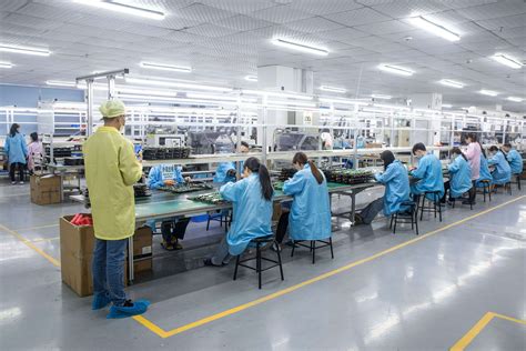
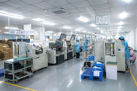
The global landscape of PCB assembly services is dominated by organizations that combine technical expertise with scalable manufacturing capabilities Companies specializing in PCBA (Printed Circuit Board Assembly) distinguish themselves through certifications like ISO 9001 and IPC-A-610, ensuring adherence to international quality benchmarks For instance, high-density interconnect (HDI) boards and flexible circuit designs are increasingly prioritized by leading providers to meet the demands of aerospace, medical devices, and IoT applications
A comparative analysis of key players reveals distinct strengths:
| Company | Headquarters | Key Offerings |
|---|---|---|
| TTM Technologies | USA | High-mix, low-volume prototyping |
| Jabil | Global | End-to-end supply chain integration |
| Sanmina | USA | Advanced RF and microwave solutions |
| Benchmark Electronics | Singapore | Miniaturized PCB assemblies |
| Celestica | Canada | Automotive-grade reliability testing |
Tip: When selecting a PCB assembly partner, verify their capacity for design-for-manufacturability (DFM) reviews This step minimizes post-production revisions and accelerates time-to-market
Regional specialization plays a critical role in supplier selection Asian-based firms often excel in cost-effective high-volume production, while North American and European providers focus on mission-critical assemblies requiring stringent compliance Emerging trends, such as the integration of AI-driven quality inspection systems, further enhance precision in solder joint analysis and component placement accuracy
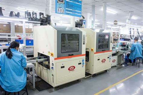
The shift toward Industry 40 has prompted PCBA leaders to adopt smart factory frameworks, leveraging IoT-enabled equipment for real-time process monitoring This transformation ensures traceability across multilayer board fabrication and final testing phases, particularly for applications in 5G infrastructure and autonomous vehicles
As supply chain complexities grow, dual sourcing strategies are becoming essential Partners with geographically distributed facilities mitigate risks associated with logistics disruptions, ensuring uninterrupted PCB assembly services for global clients
Advanced PCB Manufacturing Solutions
The evolution of PCB assembly has been driven by the demand for miniaturization, higher signal integrity, and multi-layered designs in modern electronics Leading PCBA providers now leverage automated optical inspection (AOI) systems, laser direct imaging (LDI), and high-density interconnect (HDI) technologies to meet these challenges These innovations enable the production of boards with trace widths as narrow as 25 microns, supporting applications in aerospace, medical devices, and 5G infrastructure
A key differentiator among top-tier manufacturers is their adoption of additive manufacturing techniques, such as inkjet printing for conductive layers, which reduces material waste by up to 40% compared to traditional subtractive methods Additionally, advanced PCB assembly workflows integrate machine learning algorithms to predict potential defects during solder paste application, achieving first-pass yield rates exceeding 993%
For high-frequency applications, companies utilize low-loss dielectric materials like Rogers 4000 series or Isola Astra MT77, paired with controlled impedance routing This ensures signal stability in RF and microwave circuits while maintaining thermal resilience Flexible and rigid-flex PCBA solutions are also gaining traction, particularly in wearable technology and automotive sensors, where durability and space constraints are critical
To address sustainability, forward-thinking manufacturers employ halogen-free laminates and lead-free solder alloys, aligning with RoHS and REACH directives Advanced PCB assembly facilities further enhance traceability through blockchain-enabled supply chain platforms, providing real-time component authentication and reducing counterfeit risks
As IoT and edge computing expand, the industry is shifting toward embedded component technology, where passive elements are buried within multilayer substrates This approach not only saves board space but also improves electrical performance by minimizing parasitic inductance—a vital advancement for next-gen AI-driven devices
Global PCB Assembly Supply Chains
Modern PCB assembly operations thrive on intricately coordinated global supply chain networks that balance cost efficiency with technical expertise Leading PCBA providers leverage geographically distributed manufacturing hubs to optimize material procurement, reduce lead times, and mitigate regional disruptions For instance, companies often source high-precision substrates from specialized Asian suppliers while partnering with North American or European facilities for mission-critical automated optical inspection (AOI) processes This multipolar production model ensures compliance with regional regulatory standards—such as IPC Class 3 for aerospace applications or RoHS directives for consumer electronics—without compromising scalability
The rise of smart logistics platforms has further refined PCB assembly workflows, enabling real-time tracking of components from IC packaging plants to final testing centers Tier-1 suppliers now integrate predictive analytics to anticipate shortages of multilayer laminates or semiconductor dies, dynamically rerouting orders through alternate vendors Such agility proves critical when serving industries like medical devices or automotive systems, where a single delayed shipment can stall entire production lines Notably, firms excelling in global PCBA coordination often maintain dual sourcing strategies for core materials like high-frequency PTFE substrates or lead-free solder alloys, reducing dependency on any single supplier
However, managing these complex networks requires addressing inherent challenges Tariff fluctuations, customs bottlenecks, and evolving sustainability mandates demand continuous adaptation Progressive PCB assembly companies address this by embedding compliance teams within key manufacturing regions—a practice that accelerates environmental certifications like ISO 14001 while streamlining cross-border documentation Additionally, investments in regional fulfillment centers across Southeast Asia, Eastern Europe, and Mexico allow faster response to localized demand spikes, particularly for rapid-turn prototyping services
As demand grows for miniaturized and IoT-enabled electronics, the interplay between advanced PCBA technologies and logistical precision will define market leadership Suppliers mastering this balance not only deliver faster time-to-market but also achieve 2% defect rates in high-volume orders—a benchmark increasingly expected in 5G infrastructure and industrial automation sectors
Precision Electronics Assembly Experts
In the realm of PCB assembly, achieving micrometer-level accuracy requires specialized expertise in handling complex designs and advanced materials Leading PCBA providers distinguish themselves through zero-defect manufacturing protocols, combining automated optical inspection (AOI) systems with AI-driven quality assurance tools These specialists employ high-density interconnect (HDI) techniques to accommodate miniaturized components, ensuring optimal performance for applications ranging from aerospace avionics to medical implants
A critical differentiator among top-tier PCB assembly companies lies in their mastery of mixed-technology assembly—seamlessly integrating surface-mount (SMT) and through-hole components within multilayer configurations Advanced thermal management solutions, including copper-filled vias and embedded heat sinks, address power density challenges in next-gen IoT devices For mission-critical systems, suppliers implement mil-spec compliant processes with full traceability from component sourcing to final testing
The shift toward Industry 40-ready production has redefined precision standards in PCBA workflows Real-time process monitoring via IoT-enabled equipment minimizes variability, while digital twin simulations validate assembly outcomes before physical prototyping Global leaders further enhance reliability through automated conformal coating systems that protect circuits from environmental stressors without compromising electrical performance
As product lifecycles accelerate, precision-focused PCB assembly services now prioritize agile manufacturing frameworks These enable rapid transitions between prototype validation and full-scale production, supported by cross-functional engineering teams adept at design-for-manufacturability (DFM) optimization Partnering with such experts ensures not only technical precision but also supply chain resilience, with dual-sourcing strategies and risk-mitigated material procurement networks

Cutting-Edge PCB Technologies 2024
The PCB assembly landscape is undergoing transformative shifts in 2024, driven by innovations that address the growing complexity of modern electronics Leading manufacturers now prioritize high-density interconnect (HDI) designs, enabling ultra-compact layouts for wearable devices and IoT systems These designs leverage advanced via-in-pad and microvia technologies, reducing signal loss while accommodating higher component densities
A key trend this year is the integration of artificial intelligence (AI) into PCBA workflows AI-driven inspection systems now achieve defect detection rates exceeding 9998%, significantly reducing rework costs Pairing this with 3D printing for rapid prototyping allows companies to iterate complex multilayer boards in days rather than weeks Notably, embedded component technology is gaining traction, with passive components like resistors and capacitors being laminated directly into substrate layers—a breakthrough for aerospace and medical device applications
Sustainability is also reshaping PCB assembly practices Manufacturers are adopting halogen-free substrates and lead-free soldering techniques to meet stringent EU RoHS 30 standards Meanwhile, advancements in thermally conductive polymers are improving heat dissipation in high-power boards, extending the lifespan of automotive and industrial electronics
For global supply chains, the adoption of digital twin simulations ensures seamless collaboration between design and production teams across continents This technology minimizes mismatches between virtual prototypes and physical PCBA outputs, accelerating time-to-market As 5G infrastructure expands, millimeter-wave-compatible materials like modified polyimide are becoming essential for RF-focused assemblies
These innovations underscore the industry’s shift toward smart manufacturing ecosystems, where precision, sustainability, and adaptability define competitive advantage The next frontier lies in merging these advancements with scalable production models—a challenge that will shape PCB assembly strategies through the decade
Reliable PCB Production Services
In today’s fast-paced electronics industry, selecting partners with reliable PCB production services is critical for ensuring product integrity and operational continuity Leading PCB assembly providers distinguish themselves through rigorous quality control frameworks, often backed by certifications such as ISO 9001 and IPC-A-610 standards These companies leverage automated optical inspection (AOI) and X-ray testing to detect microscopic defects in PCBA units, minimizing failure risks in end-use environments
A cornerstone of dependable production lies in scalable manufacturing ecosystems Top-tier suppliers integrate just-in-time inventory management with flexible batch processing, accommodating both low-volume prototyping and high-volume runs without compromising turnaround times This agility is particularly vital for industries like automotive and medical devices, where precision and compliance are non-negotiable
Moreover, robust supply chain resilience ensures consistent material sourcing, even during global disruptions By partnering with certified raw material vendors and maintaining multi-regional production hubs, premier PCB assembly firms mitigate risks associated with geopolitical or logistical challenges Advanced providers further enhance reliability through real-time production tracking systems, offering clients full visibility into manufacturing milestones
For businesses prioritizing longevity, PCBA specialists employ conformal coating and advanced encapsulation techniques to protect boards from environmental stressors like moisture, dust, and temperature fluctuations These value-added services extend product lifespans while reducing long-term maintenance costs
Ultimately, reliable PCB production services blend technical expertise with operational transparency, fostering trust across iterative design cycles and mass production phases By aligning with partners that prioritize both precision and adaptability, companies can navigate evolving market demands while maintaining stringent quality benchmarks
Innovative PCB Assembly Processes
The evolution of PCB assembly techniques has become a cornerstone for meeting the demands of modern electronics, particularly as devices grow more compact and functionally complex Leading manufacturers now integrate additive manufacturing methods, such as 3D-printed circuitry, to enable rapid prototyping while minimizing material waste These advanced approaches complement traditional PCBA workflows, offering unparalleled flexibility in designing high-density interconnect (HDI) boards for applications ranging from IoT devices to aerospace systems
A critical innovation lies in laser-assisted assembly, which enhances precision when mounting microcomponents like 01005-sized passives or ultra-fine-pitch BGAs This technology reduces thermal stress during soldering, improving reliability for mission-critical assemblies Simultaneously, the adoption of embedded component technology allows passive components to be layered within the substrate itself, freeing surface space for active components and enabling sleeker end-product designs
Intelligent automation has further transformed PCB assembly lines Robotic systems equipped with machine vision now handle component placement at accuracies exceeding 25µm, paired with AI-driven quality control algorithms that detect soldering defects in real time For high-mix production environments, adaptive manufacturing platforms dynamically adjust workflows based on design specifications, ensuring optimal throughput without compromising on the stringent tolerances required for automotive or medical-grade assemblies
The shift toward IoT-enabled manufacturing also plays a pivotal role Sensors embedded throughout PCBA facilities collect terabytes of process data, enabling predictive maintenance and yield optimization through advanced analytics This digital thread not only accelerates time-to-market but also strengthens traceability—a non-negotiable requirement for industries like defense and telecommunications
Emerging sustainability practices are reshaping material choices, with biodegradable substrates and lead-free solder alloys gaining traction These innovations align with global regulations while maintaining the electrical performance standards demanded by cutting-edge applications As hybrid manufacturing models blend subtractive and additive processes, the industry moves closer to achieving true zero-defect manufacturing—a critical milestone for next-generation PCB assembly ecosystems
By harmonizing these advancements, manufacturers address the dual challenges of miniaturization and functional complexity, ensuring that PCBA solutions remain at the forefront of technological progress The integration of smart factories and eco-conscious practices underscores a broader transformation—one where innovation isn’t merely additive but fundamentally redefines what’s achievable in electronics manufacturing

Leading PCB Prototyping Companies
In the realm of PCB assembly, prototyping serves as the critical bridge between design validation and full-scale production Companies specializing in PCBA prototyping distinguish themselves through rapid iteration capabilities, precision engineering, and seamless integration with advanced manufacturing workflows These firms leverage cutting-edge technologies such as high-density interconnect (HDI) layouts and multilayer flex-rigid designs to address evolving demands for miniaturization and performance optimization in sectors like aerospace, medical devices, and IoT
A hallmark of top-tier prototyping providers is their ability to deliver functional prototypes within 48–72 hours, enabling clients to accelerate product development cycles without compromising on quality Advanced facilities often incorporate automated optical inspection (AOI) systems and 3D solder paste testing to ensure compliance with IPC-A-610 standards Moreover, partnerships with global component suppliers allow these companies to mitigate supply chain risks, even when prototyping complex boards requiring specialized materials like high-frequency laminates or ceramic substrates
Transitioning from prototyping to mass production is streamlined through unified PCB assembly platforms, where design files and testing protocols are directly transferred to high-volume manufacturing lines This continuity reduces time-to-market while maintaining consistency in signal integrity and thermal management—critical factors for next-gen applications Leading players also offer design-for-manufacturability (DFM) feedback during the prototyping phase, preemptively addressing potential bottlenecks in later stages of PCBA scaling
As industries push toward smarter, more interconnected systems, the role of prototyping specialists continues to expand Their expertise in balancing speed, precision, and adaptability positions them as indispensable partners in transforming conceptual designs into market-ready PCB assembly solutions
Conclusion
Selecting the right partner for PCB assembly and PCBA services is a strategic decision that directly impacts the success of advanced electronics projects The companies highlighted in this article demonstrate how precision manufacturing, agile production frameworks, and next-generation technologies converge to address the demands of modern industries As the complexity of electronic devices grows, so does the need for PCB assembly providers capable of integrating high-density interconnect (HDI) designs, flexible substrates, and IoT-ready solutions into their workflows
A critical differentiator among leading PCBA specialists lies in their ability to balance scalability with customization While some excel in high-volume manufacturing for consumer electronics, others focus on low-volume, high-mix production for aerospace or medical devices This adaptability ensures that businesses across sectors can access supply chain resilience without compromising on technical specifications or regulatory compliance
The evolution of PCB assembly methodologies—from automated optical inspection (AOI) to 3D solder paste inspection (SPI)—underscores the industry’s commitment to near-zero defect rates Furthermore, partnerships with component sourcing networks and testing-certification bodies have become indispensable for maintaining product integrity across global markets
As we look toward 2024 and beyond, the convergence of artificial intelligence in process optimization and sustainable manufacturing practices will likely redefine benchmarks for PCBA excellence Enterprises prioritizing collaborations with technically adept, environmentally conscious PCB assembly partners position themselves to navigate both current challenges and future innovations in electronics manufacturing
Frequently Asked Questions
What services do leading PCB assembly companies typically offer?
Top providers specialize in PCBA (Printed Circuit Board Assembly), including surface-mount technology (SMT), through-hole assembly, prototyping, and full-turnkey solutions Many also offer design validation, component sourcing, and post-assembly testing to ensure compliance with industry standards
How do I choose a PCB assembly partner for complex projects?
Prioritize firms with certifications like ISO 9001 and IPC-A-610, which guarantee adherence to quality benchmarks Evaluate their expertise in handling high-density interconnect (HDI) designs, flexible PCBs, and mixed-technology assemblies Scalability and global supply chain transparency are equally critical for advanced electronics
What advancements are shaping PCB technologies in 2024?
Innovations like automated optical inspection (AOI) systems, IoT-enabled production tracking, and AI-driven defect detection are revolutionizing PCBA workflows Companies investing in 3D printing for prototyping and ultra-fine-pitch soldering techniques are gaining a competitive edge
Can PCB assembly providers manage low-volume prototyping and high-volume production?
Yes, most top-tier companies offer flexible scaling Look for suppliers with dedicated rapid prototyping lines and partnerships with component distributors to minimize lead times For mass production, verify their factory capacity and Just-In-Time (JIT) inventory systems
What quality assurance measures are standard in PCBA services?
Reputable firms implement in-circuit testing (ICT), X-ray inspection, and functional testing protocols Environmental stress screening (ESS) and cross-sectional analysis are often used for mission-critical applications like aerospace or medical devices
Explore Custom PCB Solutions Today
For tailored PCB assembly services that align with your project’s technical demands, please click here to connect with specialists offering end-to-end support from design to delivery