PCB Components Assembly: A Comprehensive Guide
Introduction
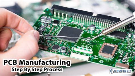
Printed Circuit Board (PCB) components assembly is a critical process in the electronics manufacturing industry. It involves the placement and soldering of electronic components onto a PCB to create a functional electronic device. The assembly process requires precision, expertise, and adherence to industry standards to ensure the reliability and performance of the final product. This article provides an in-depth overview of PCB components assembly, covering the key steps, technologies, and considerations involved in the process.
1. Overview of PCB Components Assembly
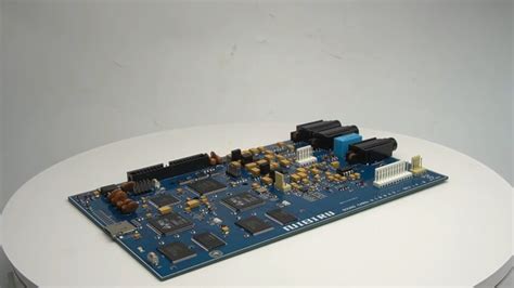
PCB components assembly, also known as PCBA (Printed Circuit Board Assembly), is the process of mounting electronic components onto a PCB. The components can be either through-hole or surface-mount devices (SMDs), and the assembly process varies depending on the type of components used. The goal of PCB assembly is to create a fully functional electronic circuit that can perform specific tasks within a device.
The assembly process typically involves the following steps:
- Component Placement: The electronic components are placed onto the PCB in their designated locations.
- Soldering: The components are soldered onto the PCB to establish electrical connections.
- Inspection and Testing: The assembled PCB is inspected and tested to ensure proper functionality and quality.
2. Types of PCB Components
There are two main types of components used in PCB assembly: through-hole components and surface-mount components.
2.1 Through-Hole Components
Through-hole components have leads that are inserted into holes drilled in the PCB. These leads are then soldered onto the opposite side of the board. Through-hole components are typically larger and more robust, making them suitable for applications that require high mechanical strength and reliability. Examples of through-hole components include connectors, large capacitors, and transformers.
2.2 Surface-Mount Components (SMDs)
Surface-mount components are smaller and are mounted directly onto the surface of the PCB. They do not require holes to be drilled in the board, which allows for higher component density and more compact designs. SMDs are widely used in modern electronics due to their small size and ability to be placed on both sides of the PCB. Examples of SMDs include resistors, capacitors, integrated circuits (ICs), and LEDs.
3. PCB Assembly Process
The PCB assembly process can be divided into several key steps, each of which plays a crucial role in ensuring the quality and functionality of the final product.
3.1 Solder Paste Application
The first step in the PCB assembly process is the application of solder paste to the PCB. Solder paste is a mixture of tiny solder particles and flux, which is applied to the pads where the components will be placed. This is typically done using a stencil that ensures the solder paste is applied only to the designated areas.
3.2 Component Placement
Once the solder paste has been applied, the next step is to place the components onto the PCB. This can be done manually for small-scale production or prototyping, but for large-scale production, automated pick-and-place machines are used. These machines use computer-controlled nozzles to pick up components from reels or trays and place them accurately onto the PCB.
3.3 Reflow Soldering
After the components have been placed, the PCB is passed through a reflow oven. The reflow oven heats the PCB to a temperature that melts the solder paste, creating a strong electrical and mechanical connection between the components and the PCB. The temperature profile in the reflow oven is carefully controlled to ensure that the solder melts evenly and that the components are not damaged by excessive heat.
3.4 Through-Hole Component Insertion
If the PCB includes through-hole components, these are inserted after the reflow soldering process. Through-hole components are typically inserted manually or using automated insertion machines. Once inserted, the leads of the components are soldered onto the PCB using wave soldering or manual soldering techniques.
3.5 Inspection and Testing
After the soldering process is complete, the assembled PCB undergoes inspection and testing to ensure that all components are correctly placed and soldered, and that the circuit functions as intended. Several inspection methods are used, including:
- Visual Inspection: A manual or automated visual inspection is performed to check for visible defects such as misaligned components, solder bridges, or insufficient solder.
- Automated Optical Inspection (AOI): AOI machines use cameras and image processing software to detect defects in the solder joints and component placement.
- X-Ray Inspection: X-ray inspection is used to inspect hidden solder joints, such as those under Ball Grid Array (BGA) components.
- Functional Testing: The assembled PCB is tested to ensure that it performs its intended function. This may involve powering up the board and running diagnostic tests.

4. Advanced PCB Assembly Technologies
As electronic devices become more complex, advanced PCB assembly technologies have been developed to meet the demands of modern electronics manufacturing.
4.1 Ball Grid Array (BGA) Assembly
BGA is a type of surface-mount packaging used for integrated circuits. BGA components have an array of solder balls on the bottom, which are used to connect the component to the PCB. BGA assembly requires precise placement and reflow soldering to ensure that the solder balls form reliable connections. X-ray inspection is often used to verify the quality of BGA solder joints.
4.2 Flexible and Rigid-Flex PCB Assembly
Flexible PCBs and rigid-flex PCBs are used in applications where the PCB needs to bend or flex during use. These types of PCBs require specialized assembly techniques to ensure that the flexible sections are not damaged during the assembly process. Components are typically placed on the rigid sections of the board, and special care is taken during soldering to avoid damaging the flexible materials.
4.3 High-Density Interconnect (HDI) PCB Assembly
HDI PCBs are used in applications where high component density and miniaturization are required. HDI PCBs have finer traces and smaller vias, which allow for more components to be placed on a smaller board. HDI assembly requires advanced placement and soldering techniques to ensure that the fine-pitch components are accurately placed and soldered.
5. Quality Control in PCB Assembly
Quality control is a critical aspect of PCB assembly, as even minor defects can lead to product failures. Several quality control measures are implemented throughout the assembly process to ensure the reliability and performance of the final product.
5.1 Design for Manufacturability (DFM)
DFM is a practice that involves designing the PCB with the assembly process in mind. This includes considering factors such as component placement, solderability, and thermal management. By designing the PCB for manufacturability, potential issues can be identified and addressed before the assembly process begins, reducing the risk of defects.
5.2 Process Control
Process control involves monitoring and controlling the various parameters of the assembly process, such as solder paste application, component placement accuracy, and reflow soldering temperature. By maintaining tight control over these parameters, manufacturers can ensure consistent quality and reduce the likelihood of defects.
5.3 Inspection and Testing
As mentioned earlier, inspection and testing are critical steps in the PCB assembly process. Automated inspection methods, such as AOI and X-ray inspection, are used to detect defects that may not be visible to the naked eye. Functional testing ensures that the assembled PCB performs its intended function and meets the required specifications.
6. Challenges in PCB Components Assembly
PCB components assembly is a complex process that presents several challenges, particularly as electronic devices become more advanced and miniaturized.
6.1 Miniaturization
As electronic devices become smaller, the components used in PCB assembly are also shrinking. This presents challenges in terms of component placement accuracy, soldering, and inspection. Advanced assembly technologies, such as HDI and BGA, are required to meet the demands of miniaturization.
6.2 Thermal Management
With the increasing power density of electronic devices, thermal management has become a critical concern in PCB assembly. Components that generate heat must be properly placed and soldered to ensure efficient heat dissipation. Thermal vias, heat sinks, and other cooling solutions are often used to manage heat in high-power applications.
6.3 Component Availability
The global supply chain for electronic components can be unpredictable, with shortages and lead times affecting the availability of certain components. Manufacturers must carefully manage their inventory and work closely with suppliers to ensure that components are available when needed.
7. Future Trends in PCB Components Assembly
The PCB components assembly industry is constantly evolving, driven by advancements in technology and the demands of new applications. Several trends are shaping the future of PCB assembly.
7.1 Automation and Robotics
Automation and robotics are playing an increasingly important role in PCB assembly. Automated pick-and-place machines, robotic soldering systems, and automated inspection systems are being used to improve efficiency, accuracy, and consistency in the assembly process.
7.2 Internet of Things (IoT) and Smart Devices
The growth of IoT and smart devices is driving demand for more complex and compact PCBs. These devices often require advanced assembly techniques, such as HDI and flexible PCB assembly, to meet the demands of miniaturization and functionality.
7.3 Green Manufacturing
Environmental concerns are driving the adoption of green manufacturing practices in PCB assembly. This includes the use of lead-free solder, recycling of materials, and reducing energy consumption during the assembly process.
Conclusion
PCB components assembly is a critical process in the electronics manufacturing industry, requiring precision, expertise, and adherence to industry standards. The assembly process involves several key steps, including solder paste application, component placement, soldering, and inspection. Advanced technologies, such as BGA assembly, flexible PCB assembly, and HDI, are being used to meet the demands of modern electronics. Quality control measures, such as DFM, process control, and inspection, are essential to ensure the reliability and performance of the final product. As the industry continues to evolve, automation, IoT, and green manufacturing are shaping the future of PCB components assembly.