Multilayer PCBs: A Comprehensive Guide to Design, Manufacturing, and Applications
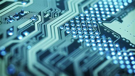
Multilayer Printed Circuit Boards (PCBs) are a cornerstone of modern electronics, enabling the development of compact, high-performance devices with complex functionality. Unlike single or double-layer PCBs, multilayer PCBs consist of three or more conductive layers separated by insulating materials, allowing for higher circuit density, improved signal integrity, and enhanced thermal management. This article provides a comprehensive guide to multilayer PCBs, covering their design principles, manufacturing processes, advantages, challenges, and applications.
1. Introduction to Multilayer PCBs
Multilayer PCBs are used in a wide range of applications, from consumer electronics to aerospace systems, where space constraints, high-speed signal requirements, and thermal management are critical. By stacking multiple layers of conductive traces and insulating materials, multilayer PCBs offer significant advantages over single or double-layer boards, including:
- Higher Circuit Density: More layers allow for more complex circuits in a smaller footprint.
- Improved Signal Integrity: Dedicated signal and ground layers reduce noise and crosstalk.
- Enhanced Thermal Management: Additional layers can be used for heat dissipation and power distribution.
2. Design Principles for Multilayer PCB
Designing a multilayer PCB requires careful consideration of electrical, thermal, and mechanical factors. Key design principles include:
2.1 Layer Stackup
The layer stackup defines the arrangement of conductive and insulating layers in the PCB. A well-designed stackup ensures optimal signal integrity, power distribution, and thermal management. Common stackup configurations include:
- Signal Layers: Used for routing high-speed signals.
- Ground and Power Planes: Provide low-impedance power distribution and reduce noise.
- Insulating Layers: Separate conductive layers and provide mechanical stability.
2.2 Signal Integrity
Signal integrity is critical in multilayer PCBs, especially for high-speed designs. Key considerations include:
- Impedance Matching: Ensure that the impedance of transmission lines matches the source and load impedances to minimize reflections.
- Trace Routing: Use controlled impedance routing for high-speed signals and minimize trace lengths to reduce signal degradation.
- Crosstalk Mitigation: Separate high-speed signal layers with ground planes to reduce crosstalk.
2.3 Power Integrity
Power integrity ensures stable and sufficient power distribution to all components. Key considerations include:
- Power Planes: Use dedicated power and ground planes to provide low-impedance power distribution.
- Decoupling Capacitors: Place decoupling capacitors close to power pins to filter noise and stabilize voltage.
- Via Placement: Use vias to connect power and ground planes, ensuring low-resistance paths.
2.4 Thermal Management
Thermal management is essential for preventing overheating and ensuring reliable operation. Key considerations include:
- Thermal Vias: Use thermal vias to transfer heat from components to the inner layers or the opposite side of the PCB.
- Copper Pour: Increase the copper area around heat-generating components to improve heat dissipation.
- Heat Sinks: Integrate heat sinks or cooling systems for high-power components.
2.5 Manufacturability
Designing for manufacturability ensures that the multilayer PCB can be produced reliably and cost-effectively. Key considerations include:
- Design Rules: Adhere to the manufacturer’s design rules for trace width, spacing, via size, and other parameters.
- Material Selection: Choose materials that are compatible with the manufacturing process and application requirements.
- Testing and Inspection: Include test points and inspection features to facilitate quality control.
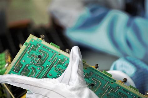
3. Manufacturing Processes for Multilayer PCBs
The manufacturing of multilayer PCBs involves several specialized processes to ensure the desired electrical, thermal, and mechanical properties. Key manufacturing steps include:
3.1 Layer Preparation
Each layer of the multilayer PCB is prepared individually by etching copper traces onto the substrate material. The layers are then laminated together under heat and pressure to form a single board.
3.2 Lamination
Lamination involves stacking the prepared layers with insulating material (prepreg) between them and applying heat and pressure to bond the layers together. The lamination process must be carefully controlled to ensure proper alignment and bonding.
3.3 Drilling and Plating
After lamination, holes are drilled through the board to create vias and through-holes. These holes are then plated with copper to establish electrical connections between layers.
3.4 Surface Finishing
A surface finish, such as electroless nickel immersion gold (ENIG) or immersion silver, is applied to protect the copper traces and enhance solderability.
3.5 Testing and Inspection
The finished multilayer PCB undergoes rigorous testing and inspection to ensure electrical performance, thermal management, and reliability. Common tests include electrical continuity testing, impedance testing, and thermal imaging.
4. Advantages of Multilayer PCBs
4.1 Higher Circuit Density
Multilayer PCBs allow for more complex circuits in a smaller footprint, enabling the development of compact and high-performance devices.
4.2 Improved Signal Integrity
Dedicated signal and ground layers reduce noise and crosstalk, ensuring reliable signal transmission in high-speed designs.
4.3 Enhanced Thermal Management
Additional layers can be used for heat dissipation and power distribution, improving thermal performance and reliability.
4.4 Reduced EMI
Proper layer stackup and grounding techniques reduce electromagnetic interference (EMI), ensuring compliance with regulatory standards.
5. Challenges of Multilayer PCBs
5.1 Complexity
Multilayer PCBs are more complex to design and manufacture than single or double-layer boards, requiring specialized knowledge and equipment.
5.2 Cost
The additional materials and manufacturing processes increase the cost of multilayer PCBs compared to simpler designs.
5.3 Manufacturing Defects
The complexity of multilayer PCBs increases the risk of manufacturing defects, such as misalignment, delamination, and via failures.
6. Applications of Multilayer PCBs
6.1 Consumer Electronics
Multilayer PCBs are used in smartphones, tablets, and laptops to enable compact and high-performance designs.
6.2 Telecommunications
High-speed and high-frequency applications, such as 5G networks and satellite systems, rely on multilayer PCBs for reliable signal transmission.
6.3 Automotive
Multilayer PCBs are used in automotive electronics, such as engine control units (ECUs) and infotainment systems, to ensure reliability and performance in harsh environments.
6.4 Aerospace and Defense
Multilayer PCBs are used in aerospace and defense systems, where reliability, performance, and compactness are critical.
6.5 Medical Devices
Multilayer PCBs are used in medical devices, such as imaging systems and implantable devices, to ensure reliability and performance in critical applications.
7. Emerging Trends in Multilayer PCBs
7.1 High-Density Interconnect (HDI)
HDI technology allows for higher component density and improved signal integrity, making it ideal for compact and high-performance designs.
7.2 Flexible and Rigid-Flex PCBs
Flexible and rigid-flex PCBs are becoming more common, offering new possibilities for compact and innovative designs.
7.3 Advanced Materials
New materials, such as high-temperature laminates and low-loss dielectrics, are being developed to improve PCB performance and reliability.
7.4 Additive Manufacturing
Additive manufacturing techniques, such as 3D printing, are being explored for creating complex PCB structures with reduced waste and cost.
8. Conclusion
Multilayer PCBs are a critical enabler of modern electronics, offering higher circuit density, improved signal integrity, and enhanced thermal management. By understanding the design principles, manufacturing processes, and challenges associated with multilayer PCBs, engineers can create high-performance and reliable electronic systems. Emerging trends, such as HDI, flexible PCBs, and advanced materials, are shaping the future of multilayer PCB technology, offering new opportunities for innovation and performance enhancement. With careful attention to detail and adherence to best practices, multilayer PCBs can deliver the reliability and performance needed to power the next generation of electronic devices.