Precision-Driven Manufacturing for Small Run PCB Assembly
Key Takeaways
When considering PCB assembly for prototyping and limited-scale production, three critical factors emerge: precision, scalability, and cost efficiency. Modern PCBA workflows leverage advanced automation and modular tooling to ensure consistent quality across low-volume batches.
"Choosing a PCB assembly partner with expertise in flexible manufacturing reduces lead times while maintaining rigorous testing protocols."
For prototyping, rapid iteration capabilities are essential. This phase benefits from:
| Aspect | Prototyping Focus | Low-Volume Emphasis |
|---|---|---|
| Production Scale | 5–50 units | 50–500 units |
| Lead Time | 24–72 hours | 5–10 business days |
| Cost per Unit | Higher (setup amortized) | Lower (bulk discounts) |
| Quality Focus | Functional validation | Reliability testing |
Small run PCB assembly excels in bridging these stages, offering cost-effective transitions from design validation to pre-production. Key considerations include:
- Advanced tech integration: Automated optical inspection (AOI) and X-ray testing in PCBA processes.
- Scalable workflows: Adaptable line configurations to accommodate design changes.
- Quality control metrics: IPC-A-610 standards compliance for solder joints and component placement.
A common pitfall is overlooking supply chain agility—opt for partners offering component sourcing support to mitigate delays. By prioritizing precision-driven methodologies, teams can optimize both prototyping speed and long-term production readiness.
Precision PCB Assembly for Prototyping
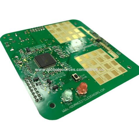
In product development, prototyping serves as the critical bridge between conceptual design and functional validation. PCB assembly for prototyping demands meticulous attention to detail, as even minor deviations can compromise performance testing. Modern low-volume prototyping workflows leverage PCBA solutions that combine automated placement systems with precision soldering techniques, ensuring repeatability across limited batches. Advanced technologies like automated optical inspection (AOI) and 3D solder paste inspection (SPI) are integrated to identify potential defects early, reducing iteration cycles.
For engineers, the ability to validate designs with functionally accurate prototypes is paramount. Specialized PCB assembly partners employ flexible manufacturing processes that accommodate design tweaks without inflating costs or timelines. This agility is particularly valuable when testing high-frequency circuits or mixed-signal boards, where material selection and trace alignment directly impact outcomes. By aligning prototyping workflows with PCBA best practices—such as design-for-manufacturing (DFM) analysis—teams can mitigate risks before scaling to production.
Moreover, prototyping-focused PCB assembly emphasizes rapid turnaround, enabling faster feedback loops. This approach not only accelerates time-to-market but also creates opportunities to refine thermal management strategies or optimize component layouts. The result is a high-fidelity prototype that mirrors final-product performance, laying a reliable foundation for subsequent manufacturing phases.
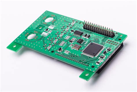
Low-Volume PCB Manufacturing Solutions
For businesses requiring PCB assembly services in limited quantities, low-volume manufacturing bridges the gap between prototyping and mass production. This approach combines the flexibility of custom PCBA with economies of scale tailored to specialized projects. Unlike traditional high-volume processes, low-volume runs prioritize rapid turnaround times and iterative design adjustments, making them ideal for R&D phases or niche applications.
Advanced manufacturers leverage automated PCB assembly lines equipped with precision pick-and-place systems and reflow soldering technology, ensuring consistent quality even for batches under 500 units. By integrating just-in-time inventory practices, suppliers minimize material waste while maintaining cost predictability. Additionally, modular production setups allow seamless transitions between different designs, supporting industries like medical devices or IoT hardware where product iterations are frequent.
Strict quality control protocols, including automated optical inspection (AOI) and functional testing, safeguard reliability in low-volume PCBA outputs. Partnering with certified manufacturers ensures compliance with industry standards such as IPC-A-610, reducing risks associated with solder joint failures or component misalignments. For startups and enterprises alike, this model balances upfront investment with scalability, enabling faster market entry without compromising on technical rigor.
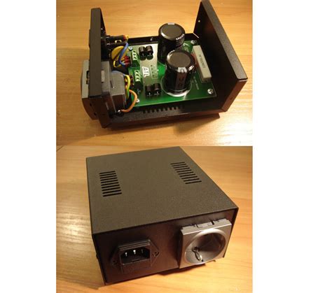
Cost-Effective Small Batch PCB Production
For businesses requiring PCB assembly services without the commitment to large-scale orders, cost-effective small batch production bridges the gap between prototyping and full-scale manufacturing. By leveraging advanced PCBA workflows, manufacturers can minimize material waste and operational overhead while maintaining precision and repeatability. Modern techniques such as automated pick-and-place systems and optimized panelization ensure efficient use of substrates, directly reducing per-unit costs for low-volume orders.
A key advantage lies in flexible pricing models tailored to small run PCB assembly, where economies of scale are redefined through modular processes and just-in-time inventory management. Designers benefit from iterative testing without incurring prohibitive expenses, enabling rapid refinements during the prototyping phase. Additionally, partnerships with specialized PCBA providers often include value-added services like design-for-manufacturing (DFM) analysis, which preemptively identifies cost drivers and optimizes layouts for material efficiency.
To further enhance affordability, manufacturers employ hybrid approaches combining surface-mount technology (SMT) and through-hole assembly based on component complexity. This strategic balance ensures high-quality outputs while avoiding unnecessary expenditures on overspecified processes. With streamlined logistics and rigorous quality control, even limited-quantity orders meet industry standards, making small batch production a viable solution for startups, R&D teams, and niche product developers.
By prioritizing scalability and resource optimization, businesses can achieve reliable PCB assembly outcomes without compromising budgetary constraints—setting the stage for seamless transitions to higher volumes as demand grows.
Advanced Tech in PCB Prototype Assembly
Modern innovations in PCB assembly are redefining the possibilities for prototyping, blending speed with uncompromising precision. The integration of automated optical inspection (AOI) systems ensures microscopic accuracy in PCBA processes, catching defects as small as 10µm during early-stage builds. Advanced pick-and-place machines equipped with machine vision now handle ultra-fine-pitch components, enabling the assembly of high-density interconnects (HDIs) critical for IoT and wearable devices.
Another breakthrough lies in the adoption of 3D printing for rapid tooling, slashing lead times for custom jigs from weeks to hours. Laser-direct imaging (LDI) further accelerates prototype iterations by eliminating photomasks, allowing engineers to test design tweaks within 24 hours. For low-volume runs, modular PCB assembly lines combine flexible robotics with adaptive process controls, maintaining consistency across batches as small as 5 units.
Emerging AI-powered analytics are transforming workflow optimization, predicting potential solder joint failures before physical testing. This synergy of PCBA technologies not only streamlines prototyping but also creates a seamless bridge to scaled production, ensuring design integrity remains intact from concept to final product.
Quality Control in Small Run PCB Builds
Maintaining rigorous quality control in small run PCB assembly is critical to ensuring reliability, even for limited production volumes. Unlike high-volume manufacturing, PCBA for prototypes or low-volume batches requires adaptable inspection protocols that balance efficiency with precision. Advanced tools like automated optical inspection (AOI) and X-ray testing are deployed to detect micro-defects, such as solder bridging or misaligned components, which are common in compact designs.
To address variability in small batch production, manufacturers implement statistical process control (SPC) methodologies. This involves real-time monitoring of critical parameters during PCB assembly, from paste application to reflow soldering, ensuring consistency across all units. For specialized applications, electrical testing—including in-circuit testing (ICT) or flying probe verification—validates functionality while minimizing post-production failures.
Material traceability is another cornerstone of quality assurance. Certified suppliers for substrates, solder masks, and components reduce risks of contamination or performance drift. Additionally, ISO 9001-compliant documentation tracks every step of the PCBA workflow, enabling rapid root-cause analysis if revisions are needed. By integrating these strategies, low-volume projects achieve first-pass yield rates comparable to mass production, aligning with the precision-driven demands of modern electronics development.
Optimizing PCB Prototyping Workflows
Efficient workflows in PCB assembly are critical for bridging the gap between design validation and full-scale production, particularly for prototyping phases. By integrating automated design-for-manufacturing (DFM) analysis tools, teams can preemptively identify layout conflicts or component placement issues, reducing iterative delays. For PCBA projects, adopting modular tooling setups allows manufacturers to swiftly reconfigure assembly lines for diverse prototype batches without compromising throughput.
Advanced real-time monitoring systems further enhance process control by tracking solder paste application, component alignment, and reflow parameters during small run PCB assembly. This data-driven approach minimizes human error while maintaining consistency across low-volume builds. Additionally, leveraging cloud-based collaboration platforms enables concurrent feedback loops between design engineers and PCBA specialists, accelerating time-to-market for prototype iterations.
To maximize cost efficiency, many providers now employ hybrid manufacturing models—combining rapid-turn PCB assembly services for critical components with standardized subassemblies. This strategy balances customization needs with economies of scale, ensuring prototypes meet functional requirements without exceeding budgetary constraints for iterative design cycles.
Benefits of Precision-Driven PCB Assembly
Precision-driven PCB assembly processes deliver measurable advantages for low-volume production, particularly in balancing technical accuracy with economic efficiency. By leveraging advanced PCBA methodologies, manufacturers minimize material waste while maintaining tight tolerances—critical for prototypes and specialized applications. Automated optical inspection (AOI) systems, paired with laser-aligned placement machinery, ensure sub-millimeter accuracy in component positioning, reducing post-production rework by up to 40%.
A key benefit lies in scalability: precision techniques originally developed for prototyping seamlessly transition to full-scale manufacturing, eliminating workflow disruptions. This adaptability is especially valuable for industries like medical devices or aerospace, where even minor deviations in PCB assembly can compromise end-product reliability. Additionally, data-driven process optimization—such as real-time thermal profiling—enhances solder joint integrity, extending the lifecycle of low-volume batches.
Cost efficiency is further amplified through modular PCBA setups, which allow rapid reconfiguration for diverse project requirements without sacrificing speed or quality. Manufacturers employing precision workflows often achieve faster time-to-market by integrating design-for-manufacturability (DFM) feedback early in the prototyping phase. Rigorous traceability protocols also simplify compliance with industry certifications, reducing audit risks for clients.
This approach not only elevates product consistency but creates a foundation for iterative innovation, enabling engineers to refine designs between production cycles without incurring prohibitive costs.
Choosing Small Run PCB Assembly Partners
Selecting the right manufacturing partner for small run PCB assembly requires balancing technical expertise, scalability, and responsiveness. Prioritize providers with proven experience in PCBA processes optimized for prototyping and low-volume batches, as these demand distinct workflows compared to mass production. Key indicators include certifications like ISO 9001 or IPC-A-610, which reflect adherence to precision and reliability standards.
Equally important is evaluating a partner’s capacity for design-for-manufacturability (DFM) feedback, ensuring your prototype aligns with production realities early in development. Transparent communication tools—such as real-time order tracking and dedicated engineering support—streamline iterations and reduce time-to-market. Additionally, assess their supply chain agility: partners with robust component sourcing networks mitigate risks of delays, even for niche materials.
Cost structures should be flexible, avoiding hidden fees for setup or tooling changes common in smaller batches. Finally, review case studies or client testimonials focused on low-volume transitions to mass production, as this reveals a partner’s ability to scale alongside your project’s growth. A collaborative approach ensures PCB assembly processes remain adaptable, cost-efficient, and quality-driven at every stage.
Conclusion
In the realm of PCB assembly, the demand for precision-driven processes in small-scale production continues to shape modern manufacturing strategies. As industries prioritize agility and customization, selecting partners specializing in PCBA for prototyping and limited-run builds becomes critical. Advanced technologies such as automated optical inspection (AOI) and surface-mount technology (SMT) ensure that even low-volume orders meet the same stringent quality benchmarks as mass-produced units. By integrating iterative design improvements directly into the manufacturing workflow, businesses can accelerate product development cycles while maintaining cost efficiency. The synergy between rigorous testing protocols and lean production methodologies not only reduces material waste but also enhances functional reliability—key factors for startups and established enterprises alike. Ultimately, leveraging tailored PCB assembly solutions empowers organizations to respond swiftly to market demands, ensuring that innovation remains both scalable and sustainable in fast-paced technological landscapes.
Frequently Asked Questions
What defines a "small run" in PCB assembly?
A small run PCB assembly typically refers to production batches ranging from 1 to 100 units. This approach prioritizes flexibility and cost efficiency, making it ideal for prototyping or niche product launches where large-scale manufacturing isn’t yet justified.
How does PCBA differ from standard PCB assembly?
PCBA (Printed Circuit Board Assembly) includes the full process of populating a bare PCB with components, whereas PCB assembly often refers to the broader manufacturing workflow. Small run PCBA emphasizes precision soldering and component placement, even at low volumes.
What quality control measures apply to low-volume production?
Advanced systems like automated optical inspection (AOI) and functional testing ensure reliability in small run PCB builds. These steps validate solder integrity, component alignment, and electrical performance, mirroring standards used in high-volume runs.
Can small batch production reduce time-to-market for prototypes?
Yes. By leveraging advanced tech in PCB prototype assembly, such as rapid-turn fabrication and modular design practices, teams can iterate designs faster and validate concepts before scaling.
How do I choose a partner for small run PCB assembly?
Prioritize vendors with expertise in low-volume optimization, transparent pricing models, and certifications like ISO 9001. Their ability to balance speed, cost, and quality is critical for prototyping success.
Explore Custom Solutions for Your Project
Ready to streamline your PCB assembly process? Click here to explore tailored PCBA services designed for prototyping and small-scale innovation.