KiCad Flex PCB: A Comprehensive Guide to Design and Implementation
Introduction
The rapid evolution of electronics has led to the development of innovative technologies that push the boundaries of traditional design and manufacturing. Among these, flexible printed circuit boards (flex PCBs) have emerged as a game-changer, enabling the creation of lightweight, compact, and highly adaptable electronic devices. KiCad, an open-source electronic design automation (EDA) software, has become a popular tool for designing flex PCBs due to its versatility, cost-effectiveness, and active community support. This article provides a comprehensive guide to designing flex PCBs using KiCad, covering the fundamentals, design considerations, workflow, and applications of this powerful combination.
What are Flex PCBs?
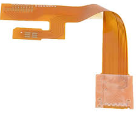
Flex PCBs, also known as flexible circuits, are a type of printed circuit board made from flexible materials such as polyimide or polyester. Unlike rigid PCBs, flex PCBs can bend, twist, and fold, making them ideal for applications where space constraints, weight reduction, and mechanical flexibility are critical. Flex PCBs are commonly used in wearable devices, medical equipment, automotive electronics, and aerospace systems.
Flex PCBs can be categorized into three main types:
- Single-Layer Flex PCBs: Consist of a single conductive layer on a flexible substrate.
- Double-Layer Flex PCBs: Feature two conductive layers with an insulating layer in between.
- Multi-Layer Flex PCBs: Comprise multiple conductive layers separated by insulating layers, offering higher complexity and functionality.
Why Use KiCad for Flex PCB Design?
KiCad is a free, open-source EDA software suite that provides a complete set of tools for designing electronic circuits and PCBs. Its features make it an excellent choice for flex PCB design:
- Cost-Effectiveness: KiCad is free to use, making it accessible to hobbyists, startups, and educational institutions.
- Cross-Platform Compatibility: KiCad runs on Windows, macOS, and Linux, ensuring broad accessibility.
- Comprehensive Toolset: KiCad includes schematic capture, PCB layout, 3D visualization, and Gerber file generation tools.
- Active Community Support: KiCad has a large and active user community that provides tutorials, forums, and plugins to enhance functionality.
- Customization: KiCad allows users to create custom footprints, symbols, and design rules, making it adaptable to specific flex PCB requirements.
Design Considerations for Flex PCBs in KiCad
Designing flex PCBs requires careful attention to mechanical, electrical, and thermal factors. Below are some key considerations when using KiCad for flex PCB design:
- Material Selection
Flex PCBs are typically made from polyimide due to its excellent thermal stability, flexibility, and mechanical strength. KiCad allows users to define custom materials and layer stack-ups to match the requirements of flex PCBs. - Bend Radius
The bend radius is the minimum radius at which a flex PCB can be bent without causing damage. KiCad’s design rule checker (DRC) can be configured to enforce bend radius constraints, ensuring the design is mechanically robust. - Trace Routing
Traces on flex PCBs should be routed to minimize stress during bending. KiCad’s interactive router and length-tuning tools help optimize trace routing for flexibility and signal integrity. - Stiffeners and Support
Stiffeners are rigid materials added to specific areas of a flex PCB to provide mechanical support for components and connectors. KiCad allows users to define stiffener regions and incorporate them into the design. - Layer Stack-Up
Flex PCBs often use a combination of flexible and rigid layers. KiCad’s layer stack-up manager enables users to define complex multi-layer configurations, including hybrid rigid-flex designs. - Thermal Management
Flex PCBs are more susceptible to thermal stress than rigid PCBs. KiCad’s thermal relief and via stitching tools help manage heat dissipation and ensure reliability. - Manufacturing Constraints
Flex PCB manufacturing requires specialized processes and tolerances. KiCad’s design rule checker can be configured to enforce manufacturing constraints, such as minimum trace width, spacing, and via size.
Workflow for Designing Flex PCBs in KiCad
The process of designing a flex PCB in KiCad involves several steps, each critical to ensuring a successful outcome. Below is an overview of the typical workflow:
- Schematic Design
The process begins with creating a schematic diagram in KiCad’s Eeschema tool. Components are placed and connected using wires and nets, defining the electrical connections of the circuit. - Component Footprints
Custom footprints for flexible components and connectors are created using KiCad’s Footprint Editor. This ensures that the footprints match the mechanical and electrical requirements of the flex PCB. - PCB Layout
The schematic is imported into KiCad’s Pcbnew tool, where the physical layout of the PCB is designed. Components are placed on the board, and traces are routed to connect them. - Layer Stack-Up Definition
The layer stack-up is defined using KiCad’s Layer Stackup Manager. For flex PCBs, this includes specifying flexible and rigid layers, as well as any stiffeners or support structures. - Routing and Optimization
Traces are routed on the flexible layers, taking care to minimize stress during bending. KiCad’s interactive router and length-tuning tools help optimize the design for flexibility and signal integrity. - Design Rule Check (DRC)
The design is checked against manufacturing and electrical rules using KiCad’s DRC tool. This ensures that the design meets all constraints and is ready for fabrication. - 3D Visualization
KiCad’s 3D viewer allows designers to visualize the flex PCB in three dimensions, ensuring that components and traces are properly placed and that the board can bend as intended. - Gerber File Generation
Once the design is finalized, Gerber files are generated using KiCad’s Plot tool. These files are sent to the PCB manufacturer for fabrication. - Testing and Validation
The fabricated flex PCB is tested to ensure it meets the required performance and reliability standards.
Advantages of Using KiCad for Flex PCB Design
KiCad offers several advantages for designing flex PCBs, making it a popular choice among engineers and hobbyists:
- Open-Source and Free
KiCad is free to use, making it accessible to a wide range of users, from hobbyists to professionals. - Customization
KiCad’s flexible design tools allow users to create custom footprints, symbols, and design rules, making it adaptable to specific flex PCB requirements. - Comprehensive Toolset
KiCad provides a complete set of tools for schematic capture, PCB layout, 3D visualization, and Gerber file generation, streamlining the design process. - Active Community Support
KiCad’s large and active user community provides tutorials, forums, and plugins to enhance functionality and troubleshoot issues. - Cross-Platform Compatibility
KiCad runs on multiple operating systems, ensuring broad accessibility and flexibility.

Applications of KiCad Flex PCBs
Flex PCBs designed using KiCad are used in a wide range of applications across various industries. Some of the most common applications include:
- Wearable Devices
Flex PCBs are ideal for wearable devices such as smartwatches, fitness trackers, and medical sensors, where flexibility and compactness are critical. - Medical Equipment
Flex PCBs are used in medical devices such as imaging systems, diagnostic equipment, and implantable devices, where reliability and miniaturization are essential. - Automotive Electronics
Flex PCBs are used in automotive applications such as infotainment systems, sensors, and lighting, where durability and space constraints are important. - Aerospace and Defense
Flex PCBs are used in avionics, radar systems, and satellite communication equipment, where lightweight and reliable performance are critical. - Consumer Electronics
Flex PCBs are used in smartphones, tablets, and laptops, where compact designs and high performance are required. - Industrial Automation
Flex PCBs are used in control systems, sensors, and robotics, where flexibility and reliability are essential.
Future Trends in KiCad Flex PCB Design
As technology continues to evolve, several trends are shaping the future of KiCad flex PCB design:
- Integration with Advanced Technologies
KiCad will play a key role in enabling emerging technologies such as IoT, 5G, and artificial intelligence, which require flexible and compact PCBs. - Enhanced Simulation Tools
The integration of advanced simulation tools into KiCad will enable more accurate modeling of flex PCB behavior under mechanical and thermal stress. - Sustainability
The electronics industry is increasingly focusing on sustainable practices, including the use of eco-friendly materials and energy-efficient designs for flex PCBs. - Automation and AI-Driven Design
The adoption of automation and AI-driven design tools will streamline the flex PCB design process, reducing development time and improving performance.
Conclusion
KiCad has emerged as a powerful and accessible tool for designing flex PCBs, enabling engineers and hobbyists to create innovative and reliable electronic devices. By understanding the design considerations, workflow, and applications of KiCad flex PCBs, users can leverage this technology to overcome the challenges of modern electronics design. As the demand for flexible and compact solutions continues to grow, KiCad will remain at the forefront of innovation, driving the development of next-generation electronic devices and shaping the future of technology.