Inlay PCB: Revolutionizing Compact and High-Density Electronics Design
In the rapidly evolving world of electronics, the demand for smaller, lighter, and more efficient devices has driven the development of innovative technologies. Among these, Inlay PCB (Printed Circuit Board) technology has emerged as a game-changer, enabling the creation of compact, high-density electronic systems. Inlay PCBs are particularly well-suited for applications where space is at a premium, such as wearable devices, medical implants, IoT (Internet of Things) devices, and advanced consumer electronics. This article explores the concept of Inlay PCBs, their design principles, manufacturing processes, applications, and the advantages they offer over traditional PCB technologies.
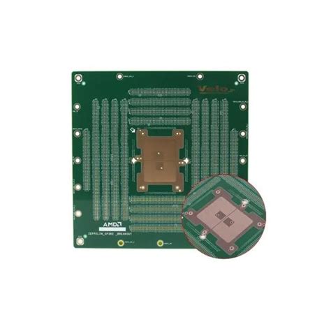
What Is an Inlay PCB?
An Inlay PCB is a specialized type of printed circuit board that integrates ultra-thin, flexible, or rigid-flex circuits into a compact form factor. The term “inlay” refers to the process of embedding or layering components and circuits within a substrate, often using advanced materials and manufacturing techniques. Inlay PCBs are designed to maximize space efficiency while maintaining high performance and reliability.
Unlike traditional PCBs, which are typically rigid and require additional space for connectors and wiring, Inlay PCBs are engineered to fit seamlessly into the design of the final product. This makes them ideal for applications where miniaturization and flexibility are critical.
Key Features of Inlay PCBs
Inlay PCBs are characterized by several unique features that set them apart from conventional PCBs:
- Ultra-Thin Design:
- Inlay PCBs are significantly thinner than traditional PCBs, often measuring less than 0.2 mm in thickness. This allows them to be integrated into tight spaces without compromising performance.
- High-Density Interconnects:
- Inlay PCBs support high-density interconnects (HDI), enabling the placement of more components and traces in a smaller area.
- Flexible and Rigid-Flex Options:
- Inlay PCBs can be designed as flexible or rigid-flex circuits, allowing them to conform to the shape of the device or enclosure.
- Embedded Components:
- Components such as resistors, capacitors, and ICs can be embedded within the substrate, reducing the overall footprint and improving reliability.
- Advanced Materials:
- Inlay PCBs often use advanced materials such as polyimide, liquid crystal polymer (LCP), and ceramic substrates to achieve superior electrical and thermal performance.
- Miniaturization:
- The compact design of Inlay PCBs enables the development of smaller and lighter devices, which is particularly important for wearable and portable electronics.
Design Principles of Inlay PCBs
Designing an Inlay PCB requires careful consideration of several factors to ensure optimal performance and manufacturability. Here are the key design principles:
1. Layer Stackup
- The layer stackup defines the arrangement of conductive and insulating layers in the PCB. For Inlay PCBs, the stackup is optimized for thinness and flexibility while maintaining signal integrity.
2. Component Placement
- Components are strategically placed to minimize space usage and optimize signal paths. Embedded components are often used to save surface area.
3. Trace Routing
- High-density interconnects require precise trace routing to avoid signal interference and ensure reliable connections. Microvias and blind vias are commonly used to connect different layers.
4. Material Selection
- The choice of substrate and conductive materials is critical for achieving the desired electrical, thermal, and mechanical properties. Polyimide and LCP are popular choices for flexible Inlay PCBs.
5. Thermal Management
- Inlay PCBs must be designed to dissipate heat effectively, especially in high-power applications. Thermal vias and heat spreaders are often incorporated into the design.
6. Mechanical Durability
- For flexible Inlay PCBs, the design must account for bending, twisting, and other mechanical stresses to ensure long-term reliability.
Manufacturing Process of Inlay PCBs
The manufacturing process for Inlay PCBs involves several advanced techniques to achieve the desired thinness, flexibility, and performance. Here’s an overview of the key steps:
1. Material Preparation
- The substrate material (e.g., polyimide or LCP) is prepared and cleaned to ensure proper adhesion of conductive layers.
2. Layer Deposition
- Conductive layers (typically copper) are deposited onto the substrate using techniques such as sputtering or electroplating.
3. Patterning and Etching
- The conductive layers are patterned using photolithography or laser direct imaging (LDI) to create the desired circuit traces. Excess material is then etched away.
4. Via Formation
- Microvias and blind vias are created using laser drilling or mechanical drilling to connect different layers of the PCB.
5. Component Embedding
- Passive and active components are embedded within the substrate using specialized techniques such as cavity formation and lamination.
6. Lamination
- Multiple layers are laminated together under heat and pressure to form a single, cohesive structure.
7. Surface Finish
- The surface of the PCB is finished with coatings such as ENIG (Electroless Nickel Immersion Gold) or HASL (Hot Air Solder Leveling) to protect the traces and improve solderability.
8. Testing and Inspection
- The finished Inlay PCB undergoes rigorous testing and inspection to ensure it meets the required specifications. This includes electrical testing, thermal testing, and visual inspection.
Applications of Inlay PCBs
Inlay PCBs are used in a wide range of applications where compactness, flexibility, and high performance are essential. Some of the most common applications include:
- Wearable Devices:
- Smartwatches, fitness trackers, and medical wearables benefit from the thin and flexible design of Inlay PCBs, which can conform to the shape of the device and withstand repeated bending.
- Medical Implants:
- Inlay PCBs are used in implantable medical devices such as pacemakers and neurostimulators, where space is limited, and reliability is critical.
- IoT Devices:
- The compact design of Inlay PCBs makes them ideal for IoT devices, which often require high functionality in a small form factor.
- Consumer Electronics:
- Smartphones, tablets, and laptops use Inlay PCBs to achieve thinner designs and integrate more features.
- Aerospace and Defense:
- Inlay PCBs are used in avionics, satellites, and military equipment, where weight and space savings are crucial.
- Automotive Electronics:
- Advanced driver-assistance systems (ADAS) and infotainment systems leverage Inlay PCBs for their compactness and reliability.
Advantages of Inlay PCBs
Inlay PCBs offer several advantages over traditional PCBs, making them a preferred choice for many applications:
- Space Efficiency:
- The ultra-thin and compact design of Inlay PCBs allows for more efficient use of space, enabling smaller and lighter devices.
- Improved Performance:
- High-density interconnects and embedded components reduce signal loss and improve electrical performance.
- Enhanced Reliability:
- Embedded components and robust materials increase the durability and reliability of Inlay PCBs, especially in harsh environments.
- Design Flexibility:
- Flexible and rigid-flex Inlay PCBs can be customized to fit the unique shape and requirements of the device.
- Cost Savings:
- While the initial cost of Inlay PCBs may be higher, their space-saving design and reduced need for additional components can lead to overall cost savings in the final product.
Challenges and Future Trends
Despite their many advantages, Inlay PCBs also present some challenges:
- Manufacturing Complexity:
- The advanced techniques and materials required for Inlay PCBs increase manufacturing complexity and cost.
- Thermal Management:
- The compact design of Inlay PCBs can make heat dissipation more challenging, especially in high-power applications.
- Material Limitations:
- The availability and cost of advanced materials such as LCP and ceramic substrates can be a limiting factor.
Future Trends:
- 3D Printing: Additive manufacturing techniques could revolutionize the production of Inlay PCBs, enabling even greater design flexibility and customization.
- Advanced Materials: The development of new materials with superior electrical and thermal properties will further enhance the performance of Inlay PCBs.
- Integration with AI and IoT: As AI and IoT technologies continue to evolve, Inlay PCBs will play a key role in enabling smarter and more connected devices.
Conclusion
Inlay PCB technology represents a significant advancement in the field of electronics, offering unparalleled space efficiency, performance, and reliability. By enabling the creation of smaller, lighter, and more flexible devices, Inlay PCBs are driving innovation across a wide range of industries, from wearable technology to aerospace.
As the demand for compact and high-density electronics continues to grow, Inlay PCBs will remain at the forefront of technological development. By addressing the challenges and leveraging the latest advancements in materials and manufacturing, designers and engineers can unlock the full potential of Inlay PCBs, paving the way for the next generation of electronic devices.