Understanding PCB Stamp Holes: Design, Functionality, and Applications
Introduction
Printed Circuit Boards (PCBs) are the backbone of modern electronics, providing the necessary platform for electrical connections between components. As the complexity of electronic devices increases, so does the need for innovative PCB design techniques. One such technique involves the use of “stamp holes,” a feature that plays a critical role in the manufacturing, assembly, and functionality of PCBs. This article delves into the concept of PCB stamp holes, exploring their design, functionality, and applications in the electronics industry.
What Are PCB Stamp Holes?
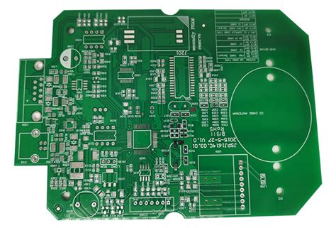
Stamp holes, also known as breakaway tabs or mouse bites, are small perforations or holes drilled along the edges of a PCB panel. These holes are strategically placed to facilitate the separation of individual PCBs from a larger panel after the manufacturing process. They are typically arranged in a line or pattern that allows for easy breaking or cutting, ensuring that the individual boards can be detached without damaging the circuitry or components.
Stamp holes are commonly used in PCB panels that contain multiple identical or different boards. These panels are manufactured as a single unit to optimize the production process, reduce material waste, and improve handling during assembly. Once the assembly process is complete, the individual boards are separated using the stamp holes.
Design Considerations for Stamp Holes
The design of stamp holes is a critical aspect of PCB manufacturing, as it directly impacts the ease of separation and the integrity of the final product. Below are some key design considerations:
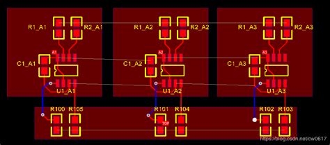
- Size and Spacing: The diameter of stamp holes typically ranges from 0.5 mm to 1.0 mm, depending on the thickness of the PCB material. The spacing between the holes is equally important, as it determines the strength of the connection between the boards. Closer spacing makes the boards easier to separate but may weaken the panel during handling.
- Placement: Stamp holes are usually placed along the edges of the PCB, near the routing or scoring lines. The placement should ensure that the separation process does not damage the circuitry or components on the board.
- Number of Holes: The number of stamp holes required depends on the size and weight of the PCB. Larger or heavier boards may require more holes to ensure a clean break.
- Material Considerations: The type of PCB material (e.g., FR-4, flexible substrates) influences the design of stamp holes. For example, flexible PCBs may require smaller or fewer holes to maintain their structural integrity.
- Manufacturing Tolerances: Designers must account for manufacturing tolerances when designing stamp holes. Misaligned or improperly sized holes can lead to difficulties during the separation process.
Functionality of Stamp Holes
Stamp holes serve several important functions in PCB manufacturing and assembly:
- Panelization: Stamp holes enable the creation of PCB panels, which are essential for mass production. By manufacturing multiple boards on a single panel, manufacturers can optimize the use of materials and reduce production costs.
- Ease of Separation: The primary function of stamp holes is to allow for the easy separation of individual boards from the panel. The perforations weaken the material along the edges, making it possible to break the boards apart without the need for complex tools.
- Mechanical Stability: During the assembly process, PCB panels must be handled and transported. Stamp holes provide a balance between stability and ease of separation, ensuring that the panels remain intact during assembly but can be easily separated afterward.
- Reduced Stress on Components: By providing a controlled breaking point, stamp holes minimize the stress on the PCB and its components during separation. This reduces the risk of damage to the circuitry or solder joints.
- Compatibility with Automated Processes: Stamp holes are compatible with automated assembly and separation processes, making them ideal for high-volume production.
Applications of Stamp Holes in PCB Design
Stamp holes are widely used in various applications across the electronics industry. Some of the most common applications include:
- Consumer Electronics: In the production of smartphones, tablets, and other consumer devices, stamp holes are used to separate multiple PCBs from a single panel. This approach is cost-effective and efficient for high-volume manufacturing.
- Industrial Electronics: Industrial control systems, sensors, and other equipment often require custom PCBs. Stamp holes enable the production of these boards in large quantities while maintaining high precision and quality.
- Automotive Electronics: The automotive industry relies on PCBs for various applications, including engine control units, infotainment systems, and sensors. Stamp holes ensure that these boards can be produced efficiently and reliably.
- Medical Devices: Medical electronics, such as imaging equipment and diagnostic tools, require high-quality PCBs. Stamp holes facilitate the production of these boards while minimizing the risk of damage during separation.
- Aerospace and Defense: In the aerospace and defense sectors, PCBs must meet stringent quality and reliability standards. Stamp holes are used to produce boards that can withstand harsh environments and rigorous testing.
Advantages of Using Stamp Holes
The use of stamp holes in PCB design offers several advantages:
- Cost Efficiency: By enabling panelization, stamp holes reduce material waste and lower production costs.
- Improved Handling: PCB panels with stamp holes are easier to handle during assembly, reducing the risk of damage or misalignment.
- Scalability: Stamp holes are ideal for high-volume production, making them suitable for industries that require large quantities of PCBs.
- Precision: The controlled separation process ensures that individual boards are free from defects and meet the required specifications.
- Versatility: Stamp holes can be used with a wide range of PCB materials and designs, making them a versatile solution for various applications.
Challenges and Limitations
While stamp holes offer numerous benefits, they also present some challenges:
- Stress Concentration: The perforations created by stamp holes can concentrate stress along the edges of the PCB, potentially leading to cracks or fractures.
- Design Complexity: Incorporating stamp holes into a PCB design requires careful planning and consideration of factors such as hole size, spacing, and placement.
- Material Limitations: Some PCB materials, such as thin or flexible substrates, may not be suitable for stamp holes due to their reduced mechanical strength.
- Post-Separation Finishing: After separation, the edges of the PCB may require additional finishing to remove burrs or sharp edges.
Best Practices for Implementing Stamp Holes
To maximize the benefits of stamp holes and minimize potential challenges, designers should follow these best practices:
- Collaborate with Manufacturers: Work closely with PCB manufacturers to ensure that the stamp hole design aligns with their capabilities and processes.
- Optimize Hole Size and Spacing: Choose hole sizes and spacing that balance ease of separation with mechanical stability.
- Use Simulation Tools: Utilize simulation tools to analyze the stress distribution and potential weak points in the PCB design.
- Conduct Prototype Testing: Test prototypes to validate the effectiveness of the stamp hole design and identify any issues before full-scale production.
- Consider Alternative Methods: In some cases, alternative methods such as V-scoring or routing may be more suitable for separating PCBs.
Conclusion
PCB stamp holes are a vital feature in modern electronics manufacturing, enabling the efficient production and separation of individual boards from larger panels. Their design and implementation require careful consideration of factors such as size, spacing, and material properties. When used correctly, stamp holes offer significant advantages, including cost efficiency, improved handling, and scalability. However, designers must also be aware of the challenges and limitations associated with stamp holes and adopt best practices to ensure optimal results.
As the electronics industry continues to evolve, the importance of innovative PCB design techniques like stamp holes will only grow. By understanding their functionality and applications, designers and manufacturers can leverage stamp holes to create high-quality, reliable PCBs that meet the demands of today’s technology-driven world.