High-Density Interconnect (HDI) Printed Circuit Boards: Revolutionizing Modern Electronics
Introduction
In the ever-evolving world of electronics, the demand for smaller, faster, and more efficient devices has driven the development of advanced printed circuit board (PCB) technologies. Among these, High-Density Interconnect (HDI) PCBs have emerged as a cornerstone in the design and manufacture of modern electronic devices. HDI PCBs are characterized by their high wiring density, which allows for more complex circuitry in a smaller footprint. This article delves into the intricacies of HDI PCBs, exploring their design, manufacturing processes, advantages, applications, and future trends.
1. Understanding HDI PCBs
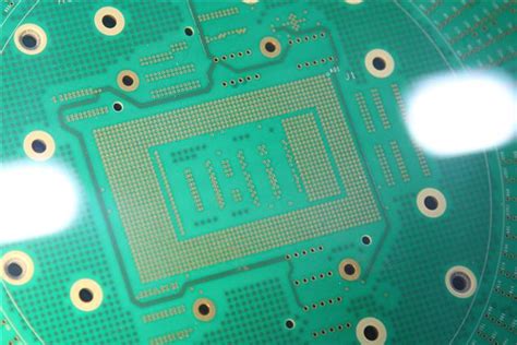
HDI PCBs are a type of printed circuit board that features a higher wiring density per unit area compared to conventional PCBs. This is achieved through the use of finer lines and spaces, smaller vias, and higher connection pad density. The primary goal of HDI technology is to enhance the electrical performance of the PCB while reducing its size and weight.
1.1 Key Features of HDI PCBs
- Microvias: One of the defining features of HDI PCBs is the use of microvias, which are small holes drilled into the PCB to connect different layers. Microvias can be as small as 50 microns in diameter, allowing for more connections in a smaller area.
- Fine Lines and Spaces: HDI PCBs utilize finer lines and spaces, often as small as 2 mils (0.002 inches) or less. This enables more complex routing and higher component density.
- Multiple Layers: HDI PCBs often have multiple layers, sometimes exceeding 20 layers, to accommodate the increased complexity of modern electronic designs.
- Blind and Buried Vias: In addition to microvias, HDI PCBs may use blind and buried vias to connect different layers without passing through the entire board. This further enhances the density and complexity of the PCB.
2. Design Considerations for HDI PCBs
Designing an HDI PCB requires careful consideration of several factors to ensure optimal performance and manufacturability.
2.1 Layer Stack-Up
The layer stack-up is a critical aspect of HDI PCB design. It involves determining the number of layers, the arrangement of signal, power, and ground layers, and the placement of microvias. A well-planned stack-up can minimize signal interference, reduce electromagnetic interference (EMI), and improve thermal management.
2.2 Signal Integrity
Signal integrity is paramount in HDI PCBs, especially in high-speed applications. Designers must consider factors such as impedance matching, crosstalk, and signal attenuation. Proper routing techniques, such as differential pair routing and controlled impedance routing, are essential to maintain signal integrity.
2.3 Thermal Management
With the increased density of components and interconnections, thermal management becomes a significant concern in HDI PCBs. Designers must ensure adequate heat dissipation through the use of thermal vias, heat sinks, and proper placement of components.
2.4 Manufacturability
Design for manufacturability (DFM) is crucial in HDI PCB design. Designers must consider the capabilities and limitations of the manufacturing process, such as the minimum feature size, via aspect ratio, and material properties. Collaboration with PCB manufacturers early in the design process can help avoid costly redesigns and ensure a smooth production process.
3. Manufacturing Process of HDI PCBs
The manufacturing process of HDI PCBs is more complex than that of conventional PCBs due to the finer features and higher layer counts. The process typically involves the following steps:
3.1 Material Selection
The choice of materials is critical in HDI PCB manufacturing. High-performance materials, such as low-loss dielectrics and high-temperature laminates, are often used to meet the demanding requirements of HDI designs.
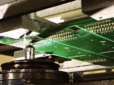
3.2 Laser Drilling
Laser drilling is used to create microvias in HDI PCBs. The precision of laser drilling allows for the creation of small, high-aspect-ratio vias that are essential for high-density interconnections.
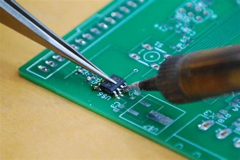
3.3 Plating and Metallization
After drilling, the vias are plated with copper to establish electrical connections between layers. This process involves several steps, including cleaning, activation, and electroless copper plating, followed by electroplating to build up the copper thickness.
3.4 Lamination
Multiple layers of the PCB are laminated together under high pressure and temperature to form a solid board. The lamination process must be carefully controlled to ensure proper alignment and bonding of the layers.
3.5 Etching and Patterning
The copper layers are etched to create the desired circuit patterns. This involves applying a photoresist, exposing it to UV light through a photomask, and then developing and etching the copper to form the traces and pads.
3.6 Surface Finish
A surface finish is applied to the PCB to protect the copper and enhance solderability. Common surface finishes for HDI PCBs include electroless nickel immersion gold (ENIG), immersion silver, and organic solderability preservatives (OSP).
3.7 Testing and Inspection
HDI PCBs undergo rigorous testing and inspection to ensure quality and reliability. This includes electrical testing, such as continuity and isolation tests, as well as visual and automated optical inspection (AOI) to detect defects.
4. Advantages of HDI PCBs
HDI PCBs offer several advantages over conventional PCBs, making them ideal for a wide range of applications.
4.1 Miniaturization
The high wiring density of HDI PCBs allows for the miniaturization of electronic devices. This is particularly important in applications such as smartphones, wearables, and medical devices, where space is at a premium.
4.2 Improved Electrical Performance
HDI PCBs offer improved electrical performance due to shorter signal paths, reduced signal loss, and lower inductance. This is critical in high-speed and high-frequency applications, such as telecommunications and data centers.
4.3 Enhanced Reliability
The use of microvias and advanced materials in HDI PCBs enhances the reliability of the board. Microvias reduce the risk of via cracking and improve thermal cycling performance, while high-performance materials provide better thermal and mechanical stability.
4.4 Cost Efficiency
While the initial cost of HDI PCBs may be higher than conventional PCBs, the overall cost efficiency is often better. The reduced size and weight of HDI PCBs can lead to savings in materials, shipping, and assembly costs. Additionally, the improved reliability can reduce the need for costly repairs and replacements.
5. Applications of HDI PCBs
HDI PCBs are used in a wide range of applications across various industries.
5.1 Consumer Electronics
HDI PCBs are widely used in consumer electronics, such as smartphones, tablets, and laptops. The miniaturization and improved performance of HDI PCBs enable the development of thinner, lighter, and more powerful devices.
5.2 Automotive
In the automotive industry, HDI PCBs are used in advanced driver-assistance systems (ADAS), infotainment systems, and engine control units (ECUs). The reliability and performance of HDI PCBs are critical in the harsh environments encountered in automotive applications.
5.3 Medical Devices
HDI PCBs are used in medical devices, such as pacemakers, imaging systems, and diagnostic equipment. The miniaturization and reliability of HDI PCBs are essential in these life-saving applications.
5.4 Aerospace and Defense
In aerospace and defense applications, HDI PCBs are used in avionics, communication systems, and radar systems. The high performance and reliability of HDI PCBs are critical in these mission-critical applications.
5.5 Industrial Equipment
HDI PCBs are used in industrial equipment, such as automation systems, robotics, and control systems. The high density and reliability of HDI PCBs enable the development of more advanced and efficient industrial systems.
6. Future Trends in HDI PCBs
The future of HDI PCBs is shaped by ongoing advancements in materials, manufacturing processes, and design techniques.
6.1 Advanced Materials
The development of advanced materials, such as low-loss dielectrics and high-temperature laminates, will continue to push the boundaries of HDI PCB performance. These materials will enable higher signal speeds, better thermal management, and improved reliability.
6.2 3D Printing
3D printing technology has the potential to revolutionize the manufacturing of HDI PCBs. By enabling the direct printing of conductive traces and vias, 3D printing could reduce the complexity and cost of HDI PCB production.
6.3 Embedded Components
The integration of embedded components, such as resistors, capacitors, and inductors, into HDI PCBs is an emerging trend. This technology can further reduce the size and weight of electronic devices while improving performance and reliability.
6.4 AI and Machine Learning
The use of AI and machine learning in PCB design and manufacturing is expected to grow. These technologies can optimize the design process, improve yield, and reduce time-to-market for HDI PCBs.
Conclusion
HDI PCBs have become an essential technology in the development of modern electronic devices. Their high wiring density, improved electrical performance, and enhanced reliability make them ideal for a wide range of applications, from consumer electronics to aerospace and defense. As advancements in materials, manufacturing processes, and design techniques continue, the future of HDI PCBs looks promising, with the potential to further revolutionize the electronics industry.