6-Layer PCB Stackup: Design, Advantages, and Applications
Printed Circuit Boards (PCBs) are the backbone of modern electronics, providing the necessary platform for mounting and interconnecting electronic components. As electronic devices become more complex, the demand for multi-layer PCBs has increased significantly. Among these, the 6-layer PCB stackup is a popular choice for many applications due to its balance between complexity, cost, and performance. This article delves into the design considerations, advantages, and typical applications of a 6-layer PCB stackup.
1. Introduction to PCB Stackup
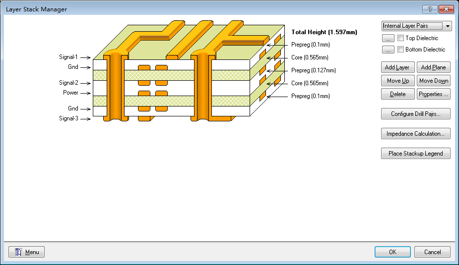
A PCB stackup refers to the arrangement of copper layers and insulating materials that make up a printed circuit board. The stackup is crucial for determining the electrical performance, signal integrity, and electromagnetic compatibility (EMC) of the PCB. A well-designed stackup can minimize crosstalk, reduce electromagnetic interference (EMI), and improve the overall reliability of the board.
2. Why Choose a 6-Layer PCB?
A 6-layer PCB offers a good compromise between the simplicity of a 4-layer board and the complexity of an 8-layer or higher layer count board. It provides additional routing layers compared to a 4-layer PCB, which is beneficial for more complex designs, while still being relatively cost-effective compared to higher layer count boards.
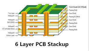
3. Typical 6-Layer PCB Stackup Configuration
A standard 6-layer PCB stackup typically consists of the following layers:
- Top Layer (Signal Layer): This is the outermost layer where most of the components are mounted. It is primarily used for routing high-speed signals and connecting components.
- Ground Plane (Inner Layer 1): This layer serves as a reference plane for the top signal layer. It helps in reducing EMI and provides a return path for high-frequency signals.
- Signal Layer (Inner Layer 2): This layer is used for routing signals that require isolation from the top and bottom layers. It is often used for medium-speed signals.
- Power Plane (Inner Layer 3): This layer is dedicated to power distribution. It provides a stable voltage reference and reduces noise in the power supply.
- Signal Layer (Inner Layer 4): Similar to Inner Layer 2, this layer is used for routing signals. It is often used for low-speed signals or signals that do not require high-speed routing.
- Bottom Layer (Signal Layer): This is the outermost layer on the opposite side of the top layer. It is used for routing signals and mounting components, similar to the top layer.
4. Design Considerations for 6-Layer PCB Stackup
Designing a 6-layer PCB stackup requires careful consideration of several factors to ensure optimal performance:
- Signal Integrity: High-speed signals should be routed on the top and bottom layers, with adjacent ground planes to minimize crosstalk and EMI. Differential pairs should be routed with consistent spacing and length matching.
- Power Integrity: The power plane should be placed close to the ground plane to form a low-impedance power distribution network (PDN). Decoupling capacitors should be placed near power pins to reduce noise.
- EMC/EMI Considerations: Proper grounding and shielding are essential to minimize EMI. The use of ground planes and careful routing of high-speed signals can help reduce EMI.
- Thermal Management: Thermal vias and proper placement of heat-generating components are important for managing heat dissipation. The power plane can also help in distributing heat.
- Manufacturability: The stackup should be designed with manufacturability in mind, considering factors such as layer thickness, material selection, and via types.
5. Advantages of a 6-Layer PCB Stackup
- Improved Signal Integrity: The additional layers allow for better isolation of high-speed signals, reducing crosstalk and improving signal integrity.
- Enhanced Power Distribution: The dedicated power plane provides a stable voltage reference and reduces noise in the power supply.
- Reduced EMI: The use of ground planes and proper routing techniques helps in minimizing EMI, making the PCB more compliant with EMC standards.
- Increased Routing Flexibility: The additional signal layers provide more routing options, making it easier to route complex designs.
- Better Thermal Management: The power plane and proper placement of thermal vias help in managing heat dissipation, improving the reliability of the PCB.
6. Applications of 6-Layer PCBs
6-layer PCBs are widely used in various applications where a balance between complexity and cost is required. Some common applications include:
- Consumer Electronics: Smartphones, tablets, and laptops often use 6-layer PCBs to accommodate the high-speed signals and complex routing required for modern electronics.
- Networking Equipment: Routers, switches, and other networking devices benefit from the improved signal integrity and reduced EMI offered by 6-layer PCBs.
- Automotive Electronics: Advanced driver-assistance systems (ADAS), infotainment systems, and engine control units (ECUs) often use 6-layer PCBs to handle the high-speed signals and power requirements.
- Industrial Control Systems: Programmable logic controllers (PLCs), motor drives, and other industrial control systems use 6-layer PCBs for their reliability and performance.
- Medical Devices: Medical imaging equipment, patient monitoring systems, and other medical devices often require the high reliability and signal integrity provided by 6-layer PCBs.
7. Conclusion
The 6-layer PCB stackup is a versatile and cost-effective solution for many modern electronic applications. Its balanced approach to signal integrity, power distribution, and EMI reduction makes it an ideal choice for complex designs that require more routing flexibility than a 4-layer PCB can offer, without the added cost and complexity of higher layer count boards. By carefully considering the design factors and following best practices, engineers can leverage the advantages of a 6-layer PCB stackup to create reliable, high-performance electronic devices.
In summary, the 6-layer PCB stackup is a powerful tool in the arsenal of PCB designers, offering a blend of performance, flexibility, and cost-effectiveness that is well-suited to a wide range of applications. As electronic devices continue to evolve, the 6-layer PCB will remain a key enabler of innovation in the electronics industry.