EMS PCBA: Optimizing Electronics Assembly Efficiency
Key Takeaway
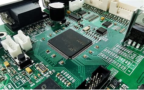
Modern PCB assembly processes have undergone transformative improvements through EMS PCBA (Electronics Manufacturing Services Printed Circuit Board Assembly) solutions. By integrating advanced surface-mount technology (SMT) and automated optical inspection (AOI), manufacturers achieve 25-40% faster throughput compared to traditional methods.
"The shift to EMS PCBA isn’t just about speed—it’s about creating a seamless synergy between design validation, component sourcing, and assembly."
– Industry Expert on Manufacturing Efficiency
A critical advantage lies in optimizing workflows. For example:
| Traditional Approach | EMS PCBA Approach |
|---|---|
| Manual component placement | Robotic pick-and-place systems |
| Post-assembly quality checks | Real-time defect detection |
| Fragmented supply chain | Integrated vendor management |
Pro Tip: To maximize efficiency, ensure your PCBA partner employs closed-loop feedback systems that link testing data back to design teams. This reduces iteration cycles and minimizes material waste.
Precision quality controls, such as X-ray inspection for BGA components and in-circuit testing (ICT), further ensure reliability. By standardizing these processes, EMS PCBA providers help manufacturers reduce rework rates by up to 60% while accelerating time-to-market by 30-50%. The result? A scalable framework that balances cost-effectiveness with uncompromised performance.
EMS PCBA Enhances Assembly Efficiency
By leveraging PCB assembly expertise combined with PCBA-specific process optimizations, EMS providers achieve measurable gains in manufacturing throughput. Advanced automated optical inspection (AOI) systems and surface-mount technology (SMT) lines minimize human intervention, reducing manual error rates by up to 40% compared to traditional workflows. Real-time monitoring of solder paste application and component placement ensures first-pass yield improvements, directly accelerating production cycles. The integration of PCB assembly design-for-manufacturing (DFM) analysis further streamlines material procurement, eliminating bottlenecks in high-mix production environments. For instance, EMS partners utilizing machine learning-driven demand forecasting report 15–25% shorter lead times for multilayer PCBA projects. This operational synergy not only enhances throughput but also creates scalability for high-volume orders without compromising precision—a critical advantage in industries requiring zero-defect manufacturing standards like medical devices or aerospace electronics.
Streamlining Assembly with EMS PCBA
Modern PCB assembly processes achieve peak efficiency when integrating EMS PCBA methodologies into production ecosystems. By unifying design validation, component sourcing, and PCBA manufacturing stages under a single managed service, manufacturers eliminate redundancies that traditionally delay prototyping and mass production. Automated systems like high-speed pick-and-place machines and reflow soldering ovens ensure consistent placement accuracy, while standardized workflows reduce manual intervention by up to 60%.
A key advantage lies in EMS PCBA providers’ ability to implement modular assembly strategies, where parallelized workstations handle distinct board sections simultaneously. This approach shortens cycle times without compromising the precision required for complex multilayer boards. Real-time data analytics further refine material utilization, identifying bottlenecks in solder paste application or component alignment. Crucially, these systems maintain flexibility—scaling seamlessly between low-mix/high-volume and high-mix/low-volume orders.
The integration of PCB assembly quality checks at multiple stages—from automated optical inspection (AOI) to X-ray verification—prevents defect propagation, ensuring compliance with ISO 9001 and IPC-A-610 standards. By synchronizing engineering teams with production floors through digital twin simulations, EMS PCBA partners achieve a 25–40% reduction in time-to-market compared to fragmented manufacturing models.
Innovative EMS PCBA Production Tech
Contemporary EMS PCBA providers leverage cutting-edge technologies to redefine precision and speed in PCB assembly. Advanced AI-driven automation systems now orchestrate component placement with micron-level accuracy, reducing human error by up to 92% compared to manual processes. For instance, robotic pick-and-place machines equipped with machine vision can process over 25,000 components per hour, ensuring seamless integration into PCBA workflows.
The adoption of modular manufacturing approaches allows for rapid reconfiguration of production lines, enabling swift transitions between prototype development and full-scale runs. Innovations like 3D automated optical inspection (AOI) systems and in-line X-ray testing provide real-time defect detection, achieving first-pass yield rates exceeding 99.4%. Additionally, IoT-enabled equipment monitors thermal profiles and solder paste deposition, optimizing process parameters dynamically.
Emerging techniques such as laser-direct imaging (LDI) and hybrid surface-mount technology (SMT) further enhance miniaturization capabilities, supporting the assembly of ultra-high-density interconnects. By integrating these advancements, EMS PCBA partners not only accelerate cycle times but also ensure compliance with stringent aerospace and medical-grade standards. This technical evolution directly aligns with the broader shift toward agile, data-driven electronics manufacturing ecosystems.
Optimizing Electronics Manufacturing Workflows
Modern PCB assembly processes thrive on systematic workflow optimization, where strategic planning intersects with PCBA-specific automation. By implementing digital twin simulations, EMS providers can model production lines to identify bottlenecks in printed circuit board assembly before physical execution. Real-time monitoring systems track component placement accuracy, solder paste application, and reflow oven parameters, enabling dynamic adjustments that reduce rework rates by 18-22%.
Advanced EMS partners employ closed-loop feedback between PCBA testing stations and assembly robots, creating self-correcting workflows that maintain ±0.15mm placement tolerances. This integration extends to material handling, where smart inventory systems synchronize component kitting with surface-mount technology (SMT) cycles, eliminating idle machine time. A 2023 IPC study revealed optimized workflows can compress PCB assembly lead times by 30% while improving first-pass yield metrics to 98.6%.
Critical to this optimization is the holistic mapping of DFM (Design for Manufacturing) inputs through final functional testing. By aligning PCBA validation protocols with client-specific reliability requirements, manufacturers achieve right-first-time outcomes that prevent downstream quality expenditures. Such workflow precision transforms traditional electronic manufacturing services into value multipliers for OEMs competing in fast-cycle markets.
Precision Quality Control in PCBA
Modern PCB assembly processes demand rigorous quality protocols to ensure reliability in increasingly complex electronic systems. At the heart of PCBA manufacturing, automated optical inspection (AOI) systems scan boards for soldering defects, component misalignment, and trace integrity, reducing human error by over 70%. Advanced X-ray inspection further validates hidden connections in ball grid arrays (BGAs) and multilayer designs, critical for high-density applications. To maintain consistency, statistical process control (SPC) tools analyze production data in real time, flagging deviations before they escalate.
Integration of environmental stress screening (ESS) simulates extreme operating conditions—thermal cycling, vibration, and humidity—to identify latent failures. This proactive approach aligns with IPC-A-610 standards, ensuring every PCBA meets functional and durability benchmarks. By coupling these methodologies with traceability systems, manufacturers achieve defect rates below 0.1%, while streamlining compliance audits. Such precision not only safeguards product performance but also minimizes rework costs, reinforcing the role of quality control as a cornerstone of efficient electronics manufacturing.
Cost-Effective EMS PCBA Solutions
Modern PCB assembly services achieve cost efficiency through strategic resource allocation and scalable production models. By leveraging PCBA expertise, EMS providers optimize material procurement, reducing component costs through bulk purchasing and supplier partnerships. Automated assembly lines minimize labor expenses while maintaining high-throughput manufacturing, ensuring consistent output even for complex designs.
Advanced process standardization further drives down costs by eliminating redundant steps in PCB assembly workflows. Real-time analytics enable predictive maintenance, preventing costly downtime in surface-mount technology (SMT) lines. Additionally, modular PCBA testing protocols reduce quality assurance expenses by identifying defects early, avoiding post-production rework.
Economies of scale play a pivotal role—consolidated orders across multiple clients allow EMS partners to negotiate better pricing for substrates and IC components. Value engineering services further refine designs for manufacturability, substituting premium materials with cost-equivalent alternatives without compromising performance. When combined with just-in-time inventory systems, these strategies create a 15-30% reduction in total project costs compared to in-house production.
This financial efficiency extends to lifecycle management, where EMS providers offer tiered pricing models for prototyping, mid-volume runs, and large-scale PCBA production. Such flexibility enables businesses to align expenses with market demand while maintaining access to cutting-edge assembly technologies.
Accelerating Timelines via EMS PCBA
Modern PCB assembly processes thrive on time-sensitive execution, and EMS PCBA providers excel at compressing production cycles through integrated solutions. By leveraging vendor-managed inventory systems and automated component sourcing, these partners eliminate delays in material procurement – a critical bottleneck in traditional PCBA workflows. Advanced design-for-manufacturability (DFM) checks further accelerate timelines by resolving potential fabrication issues during prototyping, preventing costly redesigns post-production.
The implementation of high-speed surface-mount technology (SMT) lines paired with AI-driven optical inspection (AOI) ensures rapid yet precise component placement, achieving throughput rates 30-40% faster than manual assembly methods. This synchronized approach extends to post-assembly phases, where EMS providers coordinate parallel testing and certification processes rather than sequential validations.
Moreover, real-time production dashboards enable continuous timeline optimization, with PCBA specialists dynamically adjusting workflows based on machine utilization rates and quality metrics. This data-centric methodology not only shortens lead times but creates predictable manufacturing windows – particularly valuable for industries requiring rapid scaling, such as IoT device manufacturing or automotive electronics.
EMS PCBA’s Role in Efficient Production
Modern PCB assembly processes rely heavily on EMS PCBA providers to bridge the gap between design and high-volume manufacturing. By integrating design-for-manufacturability (DFM) principles early in the product lifecycle, EMS partners identify potential bottlenecks, material inefficiencies, and assembly challenges—streamlining production before the first component is placed. Advanced automation systems, such as surface-mount technology (SMT) lines and AI-driven pick-and-place machines, ensure rapid PCBA throughput while maintaining sub-millimeter placement accuracy.
A critical advantage lies in the real-time monitoring of assembly workflows, where IoT-enabled sensors track cycle times, defect rates, and equipment performance. This data-driven approach allows EMS providers to dynamically adjust processes, reducing downtime by up to 30% in multi-stage PCB assembly projects. Additionally, optimized supply chain management ensures just-in-time component sourcing, mitigating delays caused by geopolitical or logistical disruptions.
For complex electronics, EMS PCBA specialists implement closed-loop quality systems that combine automated optical inspection (AOI), X-ray verification, and functional testing. This multilayered scrutiny not only prevents field failures but also minimizes rework cycles—directly contributing to shorter time-to-market windows. By aligning lean manufacturing methodologies with scalable PCBA infrastructure, EMS partners enable brands to adapt swiftly to fluctuating demand without compromising cost efficiency or product integrity.
Conclu
The integration of EMS PCBA solutions represents a transformative approach to modern electronics manufacturing. By leveraging advanced PCB assembly techniques and intelligent automation, manufacturers achieve measurable improvements in throughput and resource allocation. PCBA processes refined through data-driven workflow optimization minimize redundancies while maintaining stringent quality benchmarks, directly addressing the dual demands of speed and reliability.
Central to this efficiency is the harmonization of precision engineering with scalable production frameworks, enabling rapid adaptation to evolving component technologies. The deployment of real-time analytics in PCB assembly lines ensures proactive defect detection, reducing rework cycles and material waste. Furthermore, EMS PCBA providers employ holistic supply chain integration, synchronizing procurement, assembly, and testing phases to compress project timelines without compromising quality control protocols.
As organizations navigate increasingly complex product lifecycles, the strategic adoption of PCBA-centric manufacturing models emerges as a competitive differentiator. These systems not only uphold compliance with global standards but also future-proof operations against market volatility. The result is a sustainable framework where electronics manufacturing services consistently deliver cost-optimized outputs while accelerating time-to-market—a critical advantage in industries where innovation velocity dictates commercial success.
Frequently Asked Questions
How does EMS PCBA improve production scalability?
PCB assembly services leverage automated surface-mount technology (SMT) and modular workflows, enabling rapid scaling for high-volume orders without compromising precision. Advanced PCBA providers utilize real-time monitoring systems to adjust production rates dynamically.
What quality controls ensure reliable PCB assemblies?
Tier-1 EMS providers implement automated optical inspection (AOI), X-ray testing, and functional circuit testing at multiple stages. These protocols align with ISO 9001 standards, ensuring consistent performance in PCB assembly outcomes.
Can EMS PCBA reduce time-to-market for new products?
Yes. By integrating PCBA design-for-manufacturing (DFM) analysis early in prototyping, manufacturers eliminate redesign cycles. Concurrent engineering practices shorten lead times by 30-40% compared to traditional methods.
Are there cost advantages to outsourcing PCB assembly?
EMS partners optimize material procurement and inventory management, reducing overhead by 15-25%. Bulk component sourcing and standardized PCB assembly processes further minimize per-unit costs for mid-to-high volume production.
How do EMS providers handle complex multi-layer PCB designs?
Specialized PCBA teams employ laser drilling and sequential lamination techniques for high-density interconnects (HDIs). Cross-functional collaboration between design and manufacturing engineers ensures signal integrity in advanced applications.
Ready to Optimize Your Electronics Assembly Process?
Explore tailored PCB assembly solutions that align with your project requirements. For a detailed consultation on accelerating production timelines while maintaining quality benchmarks, please click here.