Optimizing PCB Assembly Factories: Advanced Techniques for Efficiency
Key Takeaways
Effective optimization of PCB assembly processes hinges on integrating cutting-edge technologies and strategic methodologies. Below are critical insights for enhancing PCBA production efficiency:
- Automation Integration: Deploying robotic placement systems and AI-driven pick-and-place machines reduces human error by 40–60%, accelerating throughput in PCB assembly workflows.
- Precision QA Protocols: Advanced inspection tools like automated optical inspection (AOI) and X-ray testing ensure 99.98% defect detection rates, safeguarding PCBA reliability.
- Lean Manufacturing: Adopting value stream mapping (VSM) eliminates 15–30% of non-value-added steps, trimming lead times and material waste.
Industry Insight: "Smart factories leveraging IoT-enabled PCB assembly lines report 25% faster response to process anomalies compared to traditional setups."
| Metric | Traditional Approach | Optimized Strategy |
|---|---|---|
| Defect Rate | 1.2% | 0.15% |
| Assembly Cycle Time | 8.5 hours | 5.2 hours |
| Inventory Turnover | 4x/year | 7x/year |
To maximize PCBA output, prioritize real-time data analytics for predictive maintenance and demand forecasting. Transitioning to modular production layouts further minimizes downtime during retooling.
Pro Tip: Pair PCB assembly automation with cross-trained personnel to maintain flexibility in high-mix, low-volume scenarios.
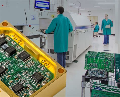
Automating PCB Assembly for Maximum Efficiency
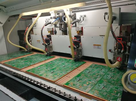
Modern PCB assembly facilities are leveraging robotic systems to achieve unprecedented levels of precision and speed. Automated pick-and-place machines now execute component placement with micron-level accuracy, reducing human error in PCBA workflows by over 70%. These systems integrate seamlessly with AI-powered vision inspection tools, enabling real-time defect detection during solder paste application and component alignment. By adopting modular automation, factories can reconfigure production lines in hours rather than days, accommodating rapid design changes common in electronics manufacturing.
Advanced conveyor systems synchronized with surface-mount technology (SMT) equipment ensure continuous material flow, minimizing bottlenecks in high-volume PCB assembly. Closed-loop feedback mechanisms automatically adjust parameters like reflow oven temperatures or placement pressure, maintaining consistent quality across batches. This automation extends to inventory management, where smart warehouses track components using RFID tags, automatically replenishing stock levels to prevent production delays.
The shift toward automation not only boosts throughput by 30–50% but also enhances traceability. Machine learning algorithms analyze production data to identify patterns, enabling predictive maintenance for critical PCBA equipment. As factories transition to lights-out manufacturing models, the integration of collaborative robots (cobots) ensures safe human-machine interaction during exception handling. These advancements lay the groundwork for leaner processes and IoT-driven optimization, creating a cohesive ecosystem where efficiency and quality coexist.
Precision QA in Modern PCB Manufacturing
Contemporary PCB assembly operations demand zero-defect approaches as component miniaturization and high-density designs become industry norms. Implementing precision QA systems now integrates automated optical inspection (AOI) and 3D X-ray verification, enabling submicron-level defect detection across PCBA boards. These systems analyze solder joint integrity, component alignment, and trace continuity at speeds exceeding 15,000 inspections/hour – a 400% efficiency gain over manual checks.
However, true quality enhancement requires data-driven feedback loops. Advanced PCB assembly factories now correlate QA metrics with production parameters using machine learning, identifying patterns like reflow oven temperature fluctuations impacting PCBA reliability. Real-time spectral analysis during wave soldering further prevents latent failures by monitoring flux activity and thermal profiles.
The transition to smart QA workflows also reduces false rejection rates below 0.2% through multi-stage validation protocols. For instance, borderline defects flagged by AOI undergo cross-verification via infrared thermal imaging before triggering rework commands. This layered approach preserves throughput while achieving first-pass yield rates above 99.4% in complex multilayer assemblies.
By embedding IoT-enabled sensors directly into conveyor systems, manufacturers achieve closed-loop process adjustments – automatically calibrating pick-and-place machines when QA data indicates component misalignment trends. Such integrations demonstrate how precision quality assurance evolves from post-production checkpoint to active process optimizer in modern electronics manufacturing ecosystems.
Lean Processes for PCB Factory Optimization
Adopting lean processes in PCB assembly operations eliminates waste while enhancing workflow precision. By analyzing production cycles through value stream mapping, factories identify bottlenecks—such as redundant material handling or idle machinery—and implement targeted improvements. For example, just-in-time (JIT) inventory systems reduce excess component stockpiling, freeing capital and minimizing storage costs. Simultaneously, standardized work instructions for PCBA technicians ensure consistent output, reducing rework rates by up to 30% in some implementations.
Integrating kaizen methodologies fosters continuous improvement, empowering teams to refine solder paste application accuracy or optimize pick-and-place machine setups. Cross-training employees across PCB assembly stages further boosts flexibility, enabling rapid response to shifting demand. Advanced analytics tools track key metrics like cycle times and defect rates, providing actionable insights for iterative refinements.
Building on advancements in automation, lean principles align seamlessly with smart factory ecosystems. Real-time data from IoT sensors, for instance, can trigger automatic replenishment of solder masks or flux, maintaining uninterrupted workflows. This synergy between lean processes and technology not only accelerates throughput but also elevates quality benchmarks, positioning PCBA facilities to meet evolving market demands efficiently.
IoT-Driven Smart PCB Assembly Lines
Integrating IoT into pcb assembly workflows is revolutionizing how factories achieve real-time visibility and adaptive production control. By embedding sensors across pcba lines, manufacturers gain granular insights into equipment performance, material flow, and environmental conditions. For instance, predictive maintenance algorithms analyze vibration and temperature data from pick-and-place machines, slashing unplanned downtime by up to 30%. These systems also enable dynamic scheduling, automatically adjusting workflows based on component availability or priority orders.
Advanced IoT platforms further enhance pcb assembly precision by correlating process data with QA outcomes. Machine learning models trained on historical defect patterns can flag anomalies in solder paste application or component alignment before batches progress. This closed-loop feedback reduces rework rates while maintaining compliance with stringent aerospace or medical-grade standards.
Moreover, cloud-based analytics unify data from distributed pcba facilities, enabling cross-site benchmarking and centralized process optimization. When paired with edge computing, latency-sensitive tasks like vision inspection achieve sub-millisecond response times. Crucially, IoT adoption aligns with lean manufacturing goals, as automated energy monitoring cuts power waste by 15–20% in high-volume lines. However, securing interconnected systems against cyberthreats remains critical, necessitating encrypted protocols and zero-trust architectures.
By bridging IoT capabilities with traditional pcb assembly infrastructure, manufacturers unlock scalable agility—a necessity in an era of shrinking product lifecycles and volatile demand.
Boosting Productivity With Advanced PCB Tech
Integrating advanced PCB assembly technologies enables manufacturers to achieve unprecedented efficiency gains. High-speed pick-and-place systems equipped with machine vision now handle PCBA components with micron-level accuracy, reducing placement errors by over 40%. Real-time process optimization powered by AI-driven algorithms dynamically adjusts parameters like solder paste application and reflow profiles, minimizing defects while accelerating cycle times.
The adoption of modular assembly lines allows PCB assembly facilities to rapidly reconfigure workflows for diverse product batches, cutting downtime by 30–50%. Additionally, edge computing devices embedded in production equipment enable predictive maintenance, identifying potential failures before they disrupt operations. These innovations not only elevate throughput but also align with lean manufacturing principles by eliminating bottlenecks.
For complex multilayer boards, laser-assisted alignment systems ensure precise layer registration, a critical factor in high-density designs. Combined with automated optical inspection (AOI), these tools slash post-assembly rework rates, ensuring faster time-to-market. By leveraging such advancements, PCBA providers can meet escalating demand without compromising quality, positioning themselves competitively in fast-paced electronics markets.
Cost-Reduction Tactics in PCB Assembly
Reducing operational expenses in PCB assembly requires a strategic balance between quality retention and cost optimization. One effective approach involves optimizing material procurement by leveraging bulk purchasing agreements or partnering with suppliers offering competitive pricing for high-grade substrates and components. Additionally, implementing lean manufacturing principles—such as minimizing material waste through precise panelization designs—can significantly lower raw material costs.
Automation plays a dual role here: integrating automated optical inspection (AOI) systems reduces labor-intensive manual checks while preventing costly rework caused by defects. For PCBA workflows, adopting modular assembly lines allows factories to scale production capacity without overinvesting in fixed assets. Energy-efficient equipment, such as low-power soldering machines, further trims utility expenses.
Another critical tactic is design for manufacturability (DFM) collaboration. By involving PCB assembly engineers early in product design, manufacturers can avoid complex layouts that increase production time and material usage. Real-time data analytics, integrated via IoT platforms, also identify bottlenecks in real-time, enabling proactive adjustments to reduce downtime.
Finally, standardizing components across projects minimizes inventory overhead and streamlines sourcing. When combined with rigorous quality assurance protocols, these strategies ensure cost reductions do not compromise the reliability of the final PCBA output.
Streamlining PCB Assembly Through Automation
Automation has become a cornerstone in modern PCB assembly workflows, enabling manufacturers to achieve unprecedented levels of speed and consistency. By integrating robotic pick-and-place systems and automated optical inspection (AOI), PCBA facilities can reduce human error while accelerating production cycles. For instance, high-speed surface-mount technology (SMT) lines now handle component placement with micron-level precision, ensuring alignment accuracy even for complex multilayer boards.
A critical advantage lies in adaptive process control, where machines self-adjust parameters like solder paste volume or reflow oven temperatures based on real-time sensor data. This minimizes defects in PCB assembly while maintaining compliance with ISO 9001 standards. Automated material handling systems further optimize workflow by synchronizing component feeders with production schedules, effectively reducing idle time between batches.
Transitioning to automated PCBA processes also supports lean manufacturing principles. Just-in-time inventory management becomes achievable through machine-to-machine communication, preventing overstocking of sensitive components like BGAs or QFNs. As factories adopt IoT-enabled equipment, data from automated systems feeds into predictive maintenance models, cutting unplanned downtime by up to 40%. These advancements create a foundation for the next logical step: implementing IoT-driven smart assembly lines, where automation and connectivity converge to deliver end-to-end traceability.
Real-Time Monitoring for Enhanced PCB Quality
Implementing real-time monitoring systems has become a cornerstone of modern PCB assembly workflows, ensuring consistent quality while minimizing production bottlenecks. By integrating IoT-enabled sensors and automated optical inspection (AOI) tools, PCBA manufacturers can track critical parameters—such as solder paste deposition accuracy, component placement alignment, and thermal profiles—during every stage of production. This data-driven approach enables immediate detection of deviations, reducing the risk of batch failures by up to 40% according to industry studies.
Advanced analytics platforms process monitoring data to identify patterns, enabling predictive adjustments to PCB assembly lines. For instance, temperature fluctuations in reflow ovens can be corrected in milliseconds, preventing solder joint defects before they occur. Additionally, machine learning algorithms refine statistical process control (SPC) models over time, optimizing tolerance thresholds for complex PCBA designs. Seamless integration with enterprise resource planning (ERP) systems further ensures traceability, allowing engineers to correlate real-time performance metrics with supplier quality data.
By prioritizing continuous feedback loops, manufacturers maintain stringent quality standards while accelerating throughput—a critical advantage in industries demanding high-reliability electronics. This synergy between precision monitoring and adaptive processes positions PCB assembly facilities to meet evolving market demands without compromising on defect rates.
Conclusion
The evolution of PCB assembly manufacturing underscores the critical balance between precision, speed, and adaptability. As demonstrated throughout this analysis, integrating automation into pcb assembly factory workflows not only accelerates production cycles but also minimizes human error, ensuring consistent output for high-volume PCBA orders. Pairing these advancements with IoT-driven monitoring creates a feedback loop where real-time data optimizes resource allocation and predictive maintenance, directly addressing bottlenecks in complex assemblies.
Equally vital is the role of lean processes in eliminating waste—whether through streamlined material handling or reduced rework rates. By embedding precision QA protocols at every stage, manufacturers safeguard product integrity while meeting stringent industry standards. These strategies collectively empower PCB assembly factories to achieve dual objectives: scaling operations without compromising quality and maintaining cost-efficiency in competitive markets.
Ultimately, the path to optimized electronics manufacturing lies in harmonizing cutting-edge technologies with methodical process refinement. For PCBA providers, this means prioritizing investments in scalable automation, data-driven decision-making, and workforce upskilling—a trifecta that future-proofs operations amid shifting consumer demands and technological advancements.
FAQs
How does automation improve efficiency in PCB assembly workflows?
Automation enhances PCBA production by minimizing manual intervention in tasks like component placement and soldering. Advanced pick-and-place systems coupled with AI-driven optical inspection can reduce error rates by over 60%, while throughput increases by 35–50% compared to semi-automated lines.
What role does precision QA play in modern PCB manufacturing?
Precision quality assurance integrates automated X-ray inspection (AXI) and in-circuit testing (ICT) to identify micro-defects in high-density boards. These systems enable real-time corrections, ensuring first-pass yield rates exceed 98% in optimized PCB assembly factories.
Can lean manufacturing principles reduce costs in PCBA production?
Yes, lean methodologies like 5S workplace organization and just-in-time inventory slashes material waste by 20–30%. Coupled with SMED (Single-Minute Exchange of Die) techniques, changeover times for PCB assembly lines drop by 40–60%, directly lowering operational expenses.
How does IoT integration benefit smart PCB factories?
IoT-enabled sensors monitor machine health and environmental conditions, predicting maintenance needs before failures occur. This reduces unplanned downtime by up to 75% in PCBA facilities while optimizing energy consumption through adaptive power management.
What strategies ensure cost-effective scaling of PCB assembly operations?
Adopting modular equipment layouts allows factories to incrementally expand capacity without full-line overhauls. Pairing this with vendor-managed inventory (VMI) systems cuts component procurement costs by 15–25%, maintaining scalability for high-mix PCB assembly demands.
Ready to Elevate Your PCB Production?
For tailored solutions in high-efficiency PCB assembly, please click here to explore advanced manufacturing strategies tailored to your operational needs.