Optimizing SMT Circuit Board Assembly for Enhanced Performance
Key Takeaways
Effective SMT circuit board optimization hinges on balancing precision, thermal control, and mechanical integrity. At the core of PCB assembly success lies precision placement strategies, which minimize component misalignment and ensure consistent electrical performance. Modern pick-and-place systems leverage vision-guided automation to achieve micron-level accuracy, critical for high-density PCBA designs.
Thermal management remains a cornerstone of reliability, with thermal profiling and material selection directly influencing heat dissipation in SMT boards. Optimizing reflow soldering parameters prevents warping and ensures uniform solder joint formation. Additionally, enhancing solder joint reliability involves rigorous inspection protocols—such as automated optical inspection (AOI)—to detect voids or cracks early in the PCB assembly process.
For high-performance electronics, integrating design-for-manufacturing (DFM) principles reduces rework and accelerates production cycles. Prioritizing solder paste stencil design and adhering to industry standards (e.g., IPC-A-610) further strengthens process consistency. By aligning these practices, manufacturers achieve durable PCBA outputs capable of withstanding mechanical stress and thermal cycling, ultimately extending product lifespans in demanding applications.
Precision SMT Placement Strategies
Achieving optimal performance in PCB assembly begins with precise component placement, a critical factor in minimizing defects and ensuring long-term reliability. Modern PCBA workflows leverage automated pick-and-place systems equipped with high-resolution vision systems to achieve placement accuracies within ±25 microns. These systems rely on advanced algorithms to align components with fiducial markers, compensating for minor board warpage or thermal expansion discrepancies.
Tip: Regularly calibrate placement machines using certified calibration standards to maintain positional accuracy, especially when handling ultra-fine-pitch components like 01005 resistors or micro-BGAs.
The selection of component libraries in assembly software plays a pivotal role. Ensuring accurate footprints and thermal profiles for each part prevents misalignment during reflow soldering. For mixed-technology boards, staggered placement sequences help avoid collisions between larger through-hole parts and delicate SMDs. Additionally, integrating real-time inspection systems, such as 3D SPI (Solder Paste Inspection), reduces risks like tombstoning or skewed orientations.
To enhance process consistency, optimize nozzle configurations for varied component sizes and prioritize feeders for high-volume parts. This minimizes machine downtime and improves throughput in high-mix PCB assembly environments. Finally, validate placement strategies through controlled prototyping runs before full-scale production, aligning with PCBA quality benchmarks for solder joint integrity and electrical performance.
By refining these strategies, manufacturers can address challenges in solder paste deposition and thermal management—key themes explored in subsequent sections.
Thermal Management for SMT Boards
Effective thermal management is critical in SMT circuit board design to prevent performance degradation and premature failure in high-power applications. As components in PCB assembly shrink in size and power density increases, managing heat dissipation becomes a balancing act between miniaturization and reliability. One proven strategy involves optimizing the PCBA layout to incorporate thermal vias and copper pours, which act as heat sinks to redistribute thermal energy away from sensitive components.
Material selection also plays a pivotal role. Using substrates with higher thermal conductivity, such as metal-core or ceramic-based boards, can significantly reduce hotspot formation. For instance, integrating thermally conductive adhesives or thermal interface materials (TIMs) between components and the board enhances heat transfer efficiency. Advanced simulation tools during the PCB assembly phase enable engineers to model thermal flow and identify potential stress points before prototyping.
Another layer of optimization involves adjusting reflow soldering profiles to minimize thermal shock while ensuring robust solder joint integrity. Controlled cooling rates and nitrogen-enriched atmospheres during soldering further mitigate oxidation risks. Post-assembly, in-circuit testing (ICT) combined with infrared thermography validates thermal performance, ensuring the PCBA meets operational thresholds for durability. By addressing these factors, manufacturers achieve stable thermal performance without compromising the compact design advantages of SMT circuit boards.

Enhancing Solder Joint Reliability
Achieving robust solder joint reliability in PCB assembly requires addressing multiple factors, from material selection to process control. Thermal cycling and mechanical stress are primary contributors to joint degradation, particularly in high-density PCBA designs. To mitigate these risks, engineers prioritize solder paste formulation with optimized alloy compositions, ensuring compatibility with both component leads and board substrates. The use of nitrogen-inerted reflow ovens further minimizes oxidation during soldering, promoting uniform wetting and reducing void formation.
Process parameters such as peak temperature and time above liquidus (TAL) must be calibrated precisely to balance intermetallic compound formation without inducing thermal damage. For mission-critical applications, post-assembly inspection via automated optical inspection (AOI) or X-ray imaging identifies microcracks or insufficient fillets before field deployment. Additionally, incorporating conformal coatings shields joints from environmental contaminants, extending operational lifespan in harsh conditions.
Aligning these strategies with thermal management practices discussed earlier ensures cohesive performance. By refining solder joint integrity, manufacturers enhance the structural stability of SMT circuit boards, directly contributing to the long-term durability of advanced electronic systems.
Efficient Circuit Board Assembly Tips
Achieving efficiency in PCB assembly requires balancing speed with precision, particularly in high-volume PCBA production. Start by optimizing component placement sequencing to minimize robotic arm movement during pick-and-place operations, which can reduce cycle times by up to 15%. Implement automated optical inspection (AOI) systems immediately after solder paste application to catch defects before reflow, preventing costly rework downstream.
Thermal management plays a dual role here: ensure reflow ovens maintain ±2°C accuracy to avoid solder bridging while accommodating board-specific thermal profiles. For mixed-technology boards, prioritize the placement of heat-sensitive components before larger parts to shield them from prolonged infrared exposure.
Leverage PCB assembly software with machine learning capabilities to predict and adjust for material expansion variances, especially in flexible substrates. When working with fine-pitch ICs, pair nitrogen-reflow environments with low-voiding solder pastes to enhance PCBA reliability. Finally, standardize feeder setups across similar product lines to cut changeover time by 30–40%, creating a repeatable workflow for high-yield manufacturing.
Advanced SMT Optimization Methods
Achieving peak performance in PCB assembly requires integrating cutting-edge techniques that address both precision and process stability. A cornerstone of advanced optimization lies in leveraging real-time feedback systems within PCBA lines, which dynamically adjust placement accuracy based on component size variations and board warpage. For high-density designs, implementing laser-assisted alignment ensures micron-level positioning of fine-pitch components like BGAs or 01005 chips, minimizing tombstoning and skew defects.
Thermal profiling also plays a pivotal role—advanced systems now employ predictive algorithms to customize reflow oven trajectories, accounting for mixed-component layouts and reducing thermal stress on sensitive parts. Additionally, adopting no-clean flux formulations with low-residue properties enhances long-term reliability while streamlining post-assembly cleaning.
To further optimize PCB assembly workflows, forward-thinking manufacturers integrate machine learning into solder paste inspection (SPI) systems. These tools analyze deposition patterns across thousands of PCBA units, identifying trends that preemptively flag potential solder joint flaws. Pairing this with modular fixture designs accelerates changeovers for mixed-product batches, maintaining throughput without compromising placement consistency. Such holistic approaches ensure that SMT processes meet the escalating demands of miniaturized, high-frequency electronics.
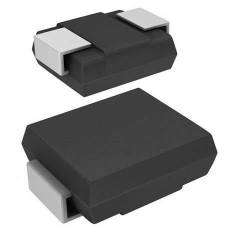
High-Performance Electronics Assembly
Modern PCB assembly processes demand meticulous attention to detail to meet the rigorous requirements of high-performance electronics. Achieving optimal results in PCBA requires balancing speed, precision, and reliability, particularly when working with densely packed SMT circuit boards. A critical factor lies in selecting automated placement systems capable of handling components as small as 01005 packages while maintaining placement accuracy within ±25µm. This precision minimizes defects and ensures consistent electrical performance across batches.
Thermal management remains a cornerstone of reliability in high-frequency applications. Engineers often integrate thermal vias and advanced substrates like polyimide or ceramic-filled laminates to dissipate heat effectively. For example:
| Parameter | Standard Assembly | High-Performance Assembly |
|---|---|---|
| Max Operating Temp | 85°C | 125°C |
| Thermal Resistance | 15°C/W | 8°C/W |
| Component Density | 25/cm² | 45/cm² |
To enhance solder joint reliability, PCBA workflows increasingly adopt nitrogen-reflow environments to reduce oxidation and improve wetting angles. Pairing this with rigorous inspection protocols, such as 3D AOI (Automated Optical Inspection), ensures even micron-level voids are detected. Additionally, low-void solder pastes and controlled ramp-to-peak profiles further mitigate thermal stress during reflow.
Finally, collaboration between design and manufacturing teams is vital. Implementing DFM (Design for Manufacturing) checks early in the PCB assembly process reduces risks of tombstoning or misalignment, particularly for fine-pitch components. By prioritizing these strategies, manufacturers can deliver SMT circuit boards that meet both performance benchmarks and long-term durability demands.
Durable SMT Board Best Practices
Achieving long-term reliability in PCB assembly requires a systematic approach to material selection, design, and process control. Start by choosing high-Tg (glass transition temperature) substrates to withstand thermal stress during PCBA reflow cycles and operational heat dissipation. Pair this with robust surface finishes like ENIG (Electroless Nickel Immersion Gold) to prevent oxidation and ensure consistent solderability.
For critical components, implement mechanical reinforcement techniques such as corner adhesives or underfill materials to mitigate vibration-induced failures. Thermal management remains pivotal—incorporate copper balancing in multilayer designs and optimize thermal via arrays to reduce hot spots that accelerate component degradation.
In PCB assembly workflows, prioritize solder paste inspection (SPI) and automated optical inspection (AOI) to detect voids or misalignments early. Use nitrogen-assisted reflow ovens to minimize oxidation during soldering, enhancing joint integrity. Post-assembly, rigorous environmental stress testing—including thermal cycling and humidity exposure—validates durability under real-world conditions.
Finally, collaborate closely with PCBA partners to standardize design-for-manufacturability (DFM) guidelines, ensuring pad geometries and stencil apertures align with solder volume requirements. By integrating these practices, manufacturers can extend the lifecycle of SMT boards while maintaining performance consistency in demanding applications.
Optimizing SMT Process Reliability
Achieving consistent reliability in SMT circuit board manufacturing demands rigorous attention to process controls and material compatibility. At the core of PCB assembly optimization lies the synchronization of solder paste application accuracy and component placement precision. Modern pick-and-place systems equipped with vision alignment technologies reduce misregistration errors below 15 microns, directly impacting PCBA longevity in high-vibration environments.
Thermal profiling remains critical, with ramp-to-peak rates requiring adjustments based on substrate thickness and component density to prevent microfractures in solder joints. Implementing nitrogen-reflow environments minimizes oxidation risks, particularly for fine-pitch components in advanced PCB assembly workflows. For mission-critical applications, accelerated life testing (ALT) validates PCBA durability under thermal cycling stresses ranging from -40°C to 125°C.
Advanced manufacturers employ statistical process control (SPC) dashboards to monitor stencil aperture fill rates and solder volume consistency—key metrics correlating with long-term SMT circuit board performance. Transitioning to low-voiding solder pastes (<5% void content) further strengthens intermetallic bonding, while conformal coating selection balances environmental protection with repairability needs. By integrating these strategies, PCBA producers systematically address failure modes linked to thermal expansion mismatches and mechanical fatigue, ensuring reliability aligns with IPC-A-610 Class 3 standards for industrial and automotive electronics.
Conclusion
As the electronics industry continues to demand higher performance and reliability, optimizing SMT circuit board assembly remains critical. By prioritizing precision placement of components and implementing robust thermal management strategies, manufacturers can significantly enhance the longevity and functionality of pcb assembly outputs. Ensuring solder joint reliability through advanced inspection techniques and material selection further mitigates failure risks in high-stress environments.
Efficient pcba workflows benefit from integrating automation and real-time monitoring, which streamline production while maintaining stringent quality standards. The adoption of predictive maintenance models and data-driven process adjustments also plays a pivotal role in minimizing downtime and defects.
Ultimately, the convergence of these methodologies not only elevates the durability of SMT boards but also aligns with the growing expectations for energy-efficient, compact electronics. As technologies evolve, continuous refinement of pcb assembly protocols will remain essential to meet the demands of next-generation applications, ensuring both performance consistency and cost-effectiveness across industries.
FAQs
What distinguishes PCB assembly from PCBA in SMT processes?
PCB assembly refers to the broader process of populating a bare circuit board, while PCBA (Printed Circuit Board Assembly) specifically denotes the completed board with all components mounted. In SMT, this distinction emphasizes the integration of surface-mount devices for compact, high-performance electronics.
How does thermal management affect SMT circuit board reliability?
Excessive heat degrades solder joints and component lifespan. Effective strategies include using thermal vias, selecting high-conductivity substrates, and implementing automated thermal profiling during PCBA to prevent warping or delamination.
What are common challenges in optimizing PCB assembly for durability?
Balancing precision placement speed with accuracy remains critical. Issues like solder bridging or tombstoning often stem from improper reflow profiles or misaligned stencils. Regular calibration of pick-and-place systems ensures consistent SMT process reliability.
Can existing PCBA designs be retrofitted for enhanced performance?
Yes. Upgrading stencil designs for finer-pitch components, adopting nitrogen-assisted reflow, and integrating real-time optical inspection (AOI) systems can modernize legacy assemblies without full redesigns.
Why is solder joint inspection vital for high-performance electronics?
Weak joints create intermittent connections, risking system failures. Combining X-ray inspection for hidden joints and automated shear testing ensures solder joint reliability in mission-critical applications.
Ready to Elevate Your SMT Assembly Workflow?
For tailored solutions in PCB assembly and PCBA optimization, please click here to consult our engineering team.
