Printed Circuit Board Etching: A Comprehensive Guide
Introduction
Printed Circuit Boards (PCBs) are the backbone of modern electronics, providing a platform for the interconnection of electronic components. The process of creating these intricate boards involves several steps, one of the most critical being the etching process. PCB etching is the method by which unwanted copper is removed from the board to create the desired circuit pattern. This article delves into the intricacies of PCB etching, exploring the various techniques, materials, and considerations involved in the process.
1. The Basics of PCB Etching
1.1. What is PCB Etching?
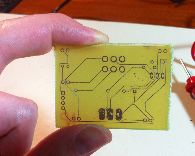
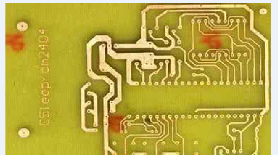
PCB etching is a subtractive manufacturing process used to remove excess copper from a PCB substrate to form the conductive pathways (traces) that connect electronic components. The process involves applying a protective layer (resist) to the copper-clad board, exposing it to a pattern (usually through a photomask), and then using a chemical solution (etchant) to dissolve the unprotected copper.
1.2. The Importance of Etching in PCB Manufacturing
Etching is crucial because it defines the electrical pathways on the PCB. The precision and quality of the etching process directly impact the performance, reliability, and functionality of the final electronic device. Poor etching can lead to short circuits, open circuits, or other electrical issues that can render the PCB useless.
2. Materials and Equipment
2.1. Substrate Materials
The most common substrate material for PCBs is FR-4, a glass-reinforced epoxy laminate. Other materials include polyimide, PTFE, and ceramic, each chosen based on the specific requirements of the application, such as thermal stability, flexibility, or high-frequency performance.
2.2. Copper Cladding
PCBs start with a copper-clad laminate, where a thin layer of copper is bonded to one or both sides of the substrate. The thickness of the copper layer can vary, typically ranging from 1 oz/ft² (35 µm) to 2 oz/ft² (70 µm), depending on the current-carrying requirements of the circuit.
2.3. Etchants
The choice of etchant is critical to the etching process. Common etchants include:
- Ferric Chloride (FeCl₃): A widely used etchant due to its effectiveness and relatively low cost. It is suitable for both hobbyist and industrial applications.
- Ammonium Persulfate: A cleaner alternative to ferric chloride, often used in industrial settings.
- Cupric Chloride (CuCl₂): Known for its ability to regenerate, making it more sustainable for large-scale production.
- Hydrochloric Acid and Hydrogen Peroxide (HCl + H₂O₂): A fast-acting etchant used in some industrial processes.
2.4. Resist Materials
The resist is a protective layer applied to the copper to prevent it from being etched away. Common resist materials include:
- Photoresist: A light-sensitive material that hardens when exposed to UV light, used in photolithography.
- Dry Film Resist: A pre-made film that is laminated onto the copper surface.
- Screen Printing Ink: A manual method where ink is applied through a mesh screen to create the resist pattern.
2.5. Equipment
The etching process requires specific equipment, including:
- Etching Tanks: Containers for holding the etchant solution, often equipped with heaters and agitation systems to improve etching uniformity.
- Developing and Etching Machines: Automated systems that handle the entire process, from applying the resist to etching and cleaning the board.
- UV Exposure Units: Used to expose the photoresist to UV light through a photomask.
- Spray Etching Machines: Use high-pressure sprays to apply the etchant, offering faster and more uniform etching.
3. The Etching Process
3.1. Preparation
Before etching, the PCB must be properly prepared. This involves cleaning the copper surface to remove any oxidation, grease, or contaminants that could interfere with the resist adhesion. Common cleaning methods include mechanical scrubbing, chemical cleaning, or plasma treatment.
3.2. Applying the Resist
The resist is applied to the copper surface to protect the areas that will form the circuit traces. The method of application depends on the type of resist used:
- Photoresist: The board is coated with a liquid photoresist, which is then dried and exposed to UV light through a photomask. The exposed areas harden, while the unexposed areas remain soluble and are washed away during development.
- Dry Film Resist: A dry film is laminated onto the copper surface, exposed to UV light, and then developed to remove the unexposed areas.
- Screen Printing: Ink is applied through a mesh screen to create the resist pattern manually.
3.3. Etching
Once the resist is applied and developed, the board is ready for etching. The etching process involves immersing the board in the etchant solution, which dissolves the unprotected copper. The key factors influencing the etching process include:
- Etchant Concentration: Higher concentrations generally result in faster etching but can lead to over-etching or undercutting.
- Temperature: Elevated temperatures increase the etching rate but can also accelerate the degradation of the resist.
- Agitation: Agitating the etchant solution helps maintain a consistent etching rate and prevents the formation of stagnant layers that can lead to uneven etching.
3.4. Stripping the Resist
After etching, the resist must be removed to reveal the copper traces. This is typically done using a chemical stripper or by mechanical means, such as scrubbing. The choice of stripper depends on the type of resist used.
3.5. Cleaning and Inspection
The final step involves cleaning the board to remove any residual etchant or resist. The board is then inspected for defects, such as incomplete etching, over-etching, or resist residues. Automated optical inspection (AOI) systems are often used in industrial settings to ensure the quality of the etched boards.
4. Advanced Etching Techniques
4.1. Laser Direct Imaging (LDI)
LDI is a modern technique that uses a laser to directly expose the photoresist, eliminating the need for a photomask. This allows for higher precision and faster turnaround times, making it ideal for high-density interconnect (HDI) PCBs.
4.2. Plasma Etching
Plasma etching is a dry etching process that uses ionized gas (plasma) to remove material. It is particularly useful for etching fine features and is often used in the production of multilayer PCBs.
4.3. Electrochemical Etching
Electrochemical etching involves using an electric current to remove copper from the PCB. This method offers precise control over the etching process and is suitable for creating very fine traces and spaces.
5. Environmental and Safety Considerations
5.1. Waste Management
The etching process generates waste materials, including spent etchant and resist residues. Proper disposal and recycling of these materials are essential to minimize environmental impact. Many etchants, such as cupric chloride, can be regenerated and reused, reducing waste.
5.2. Safety Precautions
Etching chemicals can be hazardous, requiring proper handling and safety measures. This includes using personal protective equipment (PPE), such as gloves and goggles, and working in well-ventilated areas or fume hoods. Spill containment and emergency response plans should also be in place.
6. Challenges and Future Trends
6.1. Miniaturization
As electronic devices continue to shrink, the demand for finer traces and smaller vias increases. This poses challenges for traditional etching methods, driving the development of advanced techniques like LDI and plasma etching.
6.2. Environmental Regulations
Stricter environmental regulations are pushing the industry towards greener etching solutions. This includes the development of less toxic etchants and more efficient recycling methods.
6.3. Automation and Industry 4.0
The integration of automation and smart manufacturing technologies (Industry 4.0) is transforming PCB etching. Automated etching machines, real-time monitoring, and data analytics are improving process control, reducing waste, and increasing throughput.
Conclusion
PCB etching is a critical step in the manufacturing of printed circuit boards, shaping the electrical pathways that enable modern electronics. The process involves a combination of materials, techniques, and equipment, each chosen to meet the specific requirements of the application. As the electronics industry continues to evolve, so too will the methods and technologies used in PCB etching, driven by the need for greater precision, efficiency, and environmental sustainability. Understanding the intricacies of PCB etching is essential for anyone involved in the design, manufacture, or repair of electronic devices.