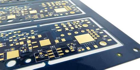
Professional 8-Layer PCB Manufacturing for High-Speed Applications

Key Takeaways
When designing 8-layer PCBs for high-speed applications, understanding core principles ensures optimal performance. Signal integrity demands controlled impedance routing and proper via placement to minimize crosstalk—critical when working with PCB manufacturing companies specializing in high-frequency boards. Effective EMI shielding often requires strategic ground plane allocation and shielding cans, particularly in dense layouts common to advanced PCB manufacturing processes.
For power distribution, consider this configuration comparison:
| Configuration | Voltage Stability | Cost Impact |
|---|---|---|
| Split Planes | High | Moderate |
| Solid Planes | Optimal | Higher |
| Hybrid Layers | Balanced | Variable |
Tip: Prioritize symmetrical stackups to reduce warping risks during fabrication—a common oversight that inflates PCB manufacturing cost.
Thermal management hinges on copper weight selection and via stitching, especially in compact designs. Precision in layer alignment (https://www.andwinpcba.com).
By aligning design choices with fabrication capabilities, you ensure reliability without compromising scalability—key when balancing performance goals with PCB manufacturing budget constraints.
Layer PCB Design Essentials
When planning multilayer PCB layouts, understanding PCB manufacturing constraints becomes critical to balancing performance and cost. Your layer stack-up configuration must account for signal integrity requirements while minimizing PCB manufacturing cost through efficient material utilization. Leading PCB manufacturing companies recommend using symmetrical layer arrangements to prevent warping—especially in designs with eight or more layers.
Key considerations include selecting dielectric materials with appropriate Dk/Df values to maintain impedance control in high-speed traces. You’ll need to prioritize power-ground layer adjacency for noise suppression, a strategy that directly impacts EMI performance. For dense layouts, microvia technology helps reduce parasitic capacitance, though it may increase PCB manufacturing business expenses due to added process complexity.
Always collaborate with your fabricator during the design phase to align trace width tolerances and via fill techniques with their capabilities. This avoids costly redesigns and ensures thermal relief patterns align with the assembly process. By integrating these principles early, you optimize both electrical performance and manufacturability, creating a foundation for reliable high-speed applications.
High-Speed Signal Integrity Solutions
When designing complex electronics for high-speed applications, maintaining signal integrity becomes critical. Controlled impedance routing and dielectric material selection directly influence how signals propagate through an 8-layer PCB, especially in environments with rapid data transfer rates. Leading PCB manufacturing companies prioritize minimizing crosstalk and reflections by optimizing trace geometry and layer stack-up configurations. For instance, placing high-speed signal layers adjacent to ground planes reduces electromagnetic interference (EMI), ensuring stable performance in dense circuits.
Balancing PCB manufacturing cost with performance requires strategic decisions. Using advanced simulation tools, engineers can predict signal behavior across different frequencies, avoiding costly redesigns. Materials like low-loss laminates (e.g., Rogers 4350B) may increase upfront expenses but significantly enhance signal clarity in high-frequency designs. Additionally, proper via placement and differential pair routing prevent impedance mismatches, which are common pain points in multilayer boards.
For businesses scaling their PCB manufacturing business, investing in precision testing equipment—such as time-domain reflectometers (TDRs)—ensures compliance with industry standards. Partnering with manufacturers skilled in PCB manufacturing for high-speed applications guarantees that your designs meet both performance benchmarks and thermal reliability requirements, seamlessly transitioning to the next phase of EMI shielding optimization.
EMI Shielding Techniques Explained
When designing an 8-layer PCB for high-speed applications, managing electromagnetic interference (EMI) is critical to ensure reliable performance. PCB manufacturing companies employ advanced techniques like ground planes and shielding cans to contain unwanted radiation. By dedicating entire layers to ground or power in the stackup, you create a Faraday cage effect, isolating sensitive signals from external noise. For example, placing high-speed traces between two ground layers minimizes crosstalk and reduces EMI emissions.
Another common approach involves using via stitching around high-frequency components or connectors. This technique connects multiple ground layers through a series of closely spaced vias, forming a low-impedance path to dissipate interference. When optimizing PCB manufacturing cost, balancing shielding effectiveness with material usage becomes essential—excessive shielding can increase layer counts or require specialized substrates.
For dense designs, PCB manufacturing experts often recommend embedded shielding materials like conductive films or ferrite sheets. These integrate seamlessly into the board structure without compromising compact layouts. Additionally, proper component placement and routing practices—such as avoiding right-angle bends—help minimize antenna effects that amplify EMI.
In high-volume PCB manufacturing business operations, automated testing tools like near-field scanners validate shielding effectiveness before mass production. By partnering with experienced manufacturers, you ensure compliance with industry standards while maintaining signal integrity and thermal stability in complex multilayer designs.

Optimized Power Layer Configurations
When designing 8-layer PCBs for high-speed applications, optimized power layer configurations become critical to balancing performance and PCB manufacturing cost. You’ll need to prioritize low-impedance power distribution networks (PDNs) to minimize voltage drops and ensure stable operation. By dedicating entire layers to power and ground planes, PCB manufacturing companies reduce electromagnetic interference (EMI) while enhancing signal integrity—key for dense circuits requiring high-speed data transfer.
Strategic placement of decoupling capacitors near power-hungry components further stabilizes voltage levels, a practice refined by experienced PCB manufacturing businesses. For multi-voltage designs, splitting power planes with proper isolation prevents crosstalk, though this requires precise layer stackup planning. Advanced simulation tools help validate configurations before fabrication, avoiding costly redesigns.
The choice of copper weight and dielectric materials also impacts thermal management and impedance control. Thicker copper layers lower resistance but increase PCB manufacturing costs, while specialized substrates improve heat dissipation in compact layouts. By collaborating with PCB manufacturing experts early, you can strike an optimal balance between performance, reliability, and budget—ensuring your design meets both technical and economic goals without compromising on power delivery efficiency.
Advanced Multilayer PCB Fabrication
When dealing with PCB manufacturing for high-layer-count designs, precision becomes non-negotiable. Advanced multilayer fabrication relies on specialized processes like laser ablation for microvia formation and sequential lamination cycles to ensure layer-to-layer registration within ±25μm tolerances. For PCB manufacturing companies, this demands not only state-of-the-art equipment but also rigorous quality protocols to prevent delamination or impedance mismatches in high-speed signal layers.
You’ll find that material selection plays a critical role here—high-performance substrates like FR-4 HT or polyimide are often paired with low-loss prepregs to maintain signal integrity across eight conductive layers. To manage PCB manufacturing cost, manufacturers optimize panel utilization and employ automated optical inspection (AOI) systems to minimize scrap rates. However, balancing cost-efficiency with performance requires expertise unique to established PCB manufacturing business operations, particularly when integrating mixed-signal layers or embedded passive components.
Modern fabrication workflows also address thermal management through advanced copper balancing and via-in-pad plating. These techniques prevent warping during reflow soldering while ensuring reliable power delivery—a necessity for applications like AI accelerators or 5G infrastructure. By partnering with PCB manufacturing companies that prioritize precision layer stacking and controlled impedance testing, you ensure your designs meet both electrical and mechanical demands without compromising scalability.
Compact Circuit Layout Strategies
Achieving compact circuit layouts in PCB manufacturing requires balancing component density with electrical performance. Start by optimizing component placement to minimize trace lengths, reducing signal delays and crosstalk—critical for high-speed applications. Use advanced design tools to automate routing, ensuring efficient use of space while adhering to impedance control requirements. For multilayer designs, strategically assign signal, power, and ground layers to avoid interference and maintain signal integrity.
When working with PCB manufacturing companies, prioritize designs that leverage stacked vias or blind/buried vias to save space without compromising reliability. However, remember that complex via structures can increase PCB manufacturing cost, so collaborate with your vendor to identify cost-effective solutions. Tight component spacing demands precise thermal management; incorporate thermal relief pads and copper pours to dissipate heat effectively.
For PCB manufacturing business clients, emphasize designs that align with scalable production processes. Avoid overly aggressive miniaturization unless necessary, as it may lead to higher defect rates. Instead, focus on standardized footprints and design-for-manufacturing (DFM) principles to ensure repeatability. By integrating these strategies, you maintain compact layouts while preserving performance and controlling costs—key priorities in modern PCB manufacturing workflows.
Ensuring PCB Thermal Reliability
When designing complex 8-layer boards for high-speed applications, managing heat dissipation becomes critical to maintaining long-term performance. PCB manufacturing processes must account for thermal expansion mismatches between materials, which can cause warping or delamination under extreme temperatures. To mitigate this, thermal vias and strategically placed copper pours help distribute heat evenly across layers, reducing hotspots that compromise reliability.
Leading PCB manufacturing companies often recommend using high-glass transition temperature (Tg) substrates, such as FR-4 HT or polyimide, to withstand repeated thermal cycling. Balancing PCB manufacturing cost with material quality is essential—opting for cost-effective laminates without sacrificing thermal resilience requires precise engineering. Additionally, incorporating dedicated power and ground planes in the stack-up minimizes resistive losses, further stabilizing thermal profiles.
For businesses scaling their PCB manufacturing business, investing in advanced thermal simulation tools ensures designs meet industry standards before fabrication. Partnering with manufacturers that offer thermal testing (e.g., infrared imaging or thermal shock tests) validates your board’s ability to handle operational stresses. By prioritizing thermal management early in the design phase, you avoid costly redesigns and ensure reliability in demanding environments.
Precision Layer Alignment Methods
Achieving registration accuracy across eight conductive layers requires specialized techniques to maintain signal integrity and prevent impedance mismatches. PCB manufacturing companies employ laser direct imaging (LDI) systems to align layers within ±25µm tolerances, ensuring precise via-to-pad connections critical for high-speed signal paths. Advanced optical registration systems track fiducial markers during lamination, compensating for thermal expansion in PCB manufacturing processes involving high-Tg materials.
For impedance-controlled designs, sequential build-up (SBU) methods enable iterative layer alignment, reducing cumulative errors that escalate PCB manufacturing cost in multilayer stacks. Automated optical inspection (AOI) validates alignment post-lamination, flagging interlayer misalignments that could compromise EMI shielding effectiveness. Tight control over dielectric thickness—down to ±3% variation—further stabilizes layer spacing, a non-negotiable parameter for power distribution networks in dense layouts.
When selecting partners for your PCB manufacturing business, prioritize facilities with X-ray layer-to-layer registration systems. These tools verify internal layer alignment non-destructively, minimizing scrap rates while maintaining the dimensional stability required for high-frequency applications. Proper alignment not only enhances signal propagation but also prevents costly re-spins caused by skewed power planes or fractured microvias.
Conclusion
When selecting PCB manufacturing partners for complex 8-layer designs, prioritizing technical expertise ensures your high-speed applications meet performance benchmarks. Reputable PCB manufacturing companies leverage advanced processes like laser-drilled microvias and sequential lamination to maintain signal integrity while minimizing crosstalk. While PCB manufacturing cost may rise with layer count and material choices, investing in precision fabrication prevents costly redesigns or field failures. For businesses scaling production, partnering with a PCB manufacturing business that offers design-for-manufacturability (DFM) feedback optimizes yield rates and reduces assembly risks.
By aligning your requirements with suppliers specializing in high-density interconnect (HDI) and thermal management, you ensure reliability under demanding conditions. Transparent communication about layer stacking, impedance control, and testing protocols helps balance PCB manufacturing cost with long-term durability. Ultimately, the right manufacturer becomes an extension of your engineering team, delivering boards that excel in EMI suppression and power efficiency—critical for next-generation electronics.

Frequently Asked Questions
How does 8-layer PCB design improve signal integrity in high-speed applications?
By dedicating specific layers to signal routing, ground planes, and power distribution, PCB manufacturing minimizes cross-talk and electromagnetic interference (EMI). Impedance-controlled traces and proper via placement further ensure stable signal transmission.
What factors influence the overall PCB manufacturing cost for 8-layer boards?
Costs depend on material selection (e.g., high-frequency laminates), layer alignment precision, and surface finishes. High-density designs requiring laser-drilled microvias or advanced EMI shielding may increase expenses, but partnering with experienced PCB manufacturing companies ensures cost-effective scaling.
Why choose specialized PCB manufacturing business providers for multilayer boards?
Expert manufacturers optimize stack-up configurations and thermal management, critical for high-speed performance. They also adhere to strict tolerances, reducing risks of delamination or misalignment—common pitfalls in complex designs.
How do I ensure reliability in compact 8-layer PCB layouts?
Prioritize symmetric layer stacking to prevent warping and use embedded passive components to save space. Collaborate with PCB manufacturing teams early to validate thermal vias and power plane designs for heat dissipation.
Can 8-layer PCBs be reworked cost-effectively?
Yes, but it requires advanced equipment and expertise. Reputable PCB manufacturing companies offer prototyping and testing phases to identify issues early, minimizing post-production revisions.
Ready to Start Your Project?
For tailored solutions in high-speed PCB manufacturing, please click here to connect with experts who optimize performance and reduce PCB manufacturing cost without compromising quality.