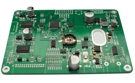
Understanding PCB Delamination: Causes, Effects, and Prevention
Printed Circuit Boards (PCBs) are the backbone of modern electronics, providing the necessary platform for electrical connections and component mounting. However, one of the critical challenges in PCB manufacturing and operation is delamination. PCB delamination refers to the separation of layers within the board, which can compromise its structural integrity and electrical performance. This article explores the causes, effects, and prevention strategies for PCB delamination.
What is PCB Delamination?
Delamination occurs when the layers of a PCB separate due to the breakdown of the adhesive material or the bonding between layers. PCBs are typically composed of multiple layers of conductive copper and insulating dielectric materials, laminated together under heat and pressure. When the bond between these layers weakens or fails, delamination occurs, leading to potential mechanical and electrical failures.
Causes of PCB Delamination
Several factors can contribute to PCB delamination, including:
- Moisture Absorption:
PCBs are often exposed to humid environments during storage or operation. Moisture can seep into the board, especially if the materials are not properly sealed. During soldering or high-temperature operations, the trapped moisture vaporizes, creating pressure that can cause layer separation. - Thermal Stress:
Excessive heat during soldering, rework, or operation can weaken the adhesive bonds between layers. Rapid temperature changes (thermal cycling) can also cause expansion and contraction, leading to delamination over time. - Poor Material Quality:
Low-quality laminate materials or improper curing of adhesives during manufacturing can result in weak interlayer bonds, making the PCB more susceptible to delamination. - Mechanical Stress:
Physical impacts, bending, or vibration during assembly or operation can cause layers to separate. - Chemical Exposure:
Exposure to harsh chemicals during cleaning or operation can degrade the adhesive properties of the PCB materials. - Manufacturing Defects:
Inadequate lamination pressure, improper curing, or contamination during the manufacturing process can lead to delamination.
Effects of PCB Delamination
Delamination can have severe consequences for the functionality and reliability of a PCB:
- Electrical Failures:
Separation of layers can disrupt electrical connections, leading to open circuits, short circuits, or intermittent connections. - Reduced Mechanical Strength:
Delamination weakens the structural integrity of the PCB, making it more prone to physical damage. - Thermal Management Issues:
Delaminated areas can trap heat, leading to localized overheating and potential component failure. - Signal Integrity Problems:
In high-frequency applications, delamination can alter the impedance of transmission lines, degrading signal quality. - Complete Board Failure:
In severe cases, delamination can render the PCB unusable, requiring costly replacements.
Prevention and Mitigation Strategies
To minimize the risk of PCB delamination, manufacturers and designers can adopt the following strategies:
- Material Selection:
Use high-quality laminate materials with low moisture absorption rates and excellent thermal stability. Ensure that the materials are compatible with the intended operating environment. - Proper Storage and Handling:
Store PCBs in a controlled environment with low humidity. Use vacuum-sealed packaging to prevent moisture absorption. - Optimized Manufacturing Processes:
Ensure proper lamination pressure, temperature, and curing times during manufacturing. Implement rigorous quality control measures to detect defects early. - Thermal Management:
Design PCBs with adequate thermal relief and heat dissipation features to minimize thermal stress. - Conformal Coating:
Apply protective coatings to shield the PCB from moisture, chemicals, and mechanical stress. - Testing and Inspection:
Conduct thorough testing, such as thermal cycling, humidity testing, and microsection analysis, to identify potential delamination issues before deployment.
Conclusion
PCB delamination is a critical issue that can significantly impact the performance and reliability of electronic devices. By understanding the causes and effects of delamination, manufacturers and designers can implement effective prevention and mitigation strategies. Through careful material selection, optimized manufacturing processes, and rigorous testing, the risk of delamination can be minimized, ensuring the longevity and reliability of PCBs in demanding applications.