Advanced Circuit Boards: Engineering Breakthroughs in Modern Electronics

Key Takeaways
Understanding core developments in PCB manufacturing helps you navigate the evolving electronics landscape. Modern precision engineering techniques enable PCB manufacturing companies to produce boards with tighter tolerances, reducing signal loss and power consumption. When assessing PCB manufacturing cost, consider how material selection (like high-frequency laminates) and automated assembly lines impact both quality and budget. For startups in the PCB manufacturing business, balancing rapid prototyping with scalable production requires strategic partnerships—domestic suppliers often provide faster iteration cycles, while offshore options may lower initial expenses.
Flex-circuit innovations and multi-layer stacking are reshaping design possibilities, but these advancements demand rigorous testing to ensure reliability. To optimize R&D timelines, prioritize vendors offering transparent communication and real-time progress tracking. By aligning your project’s complexity with the right manufacturing approach, you can mitigate risks and accelerate time-to-market for next-gen devices.
Advanced Circuit Board Design Innovations
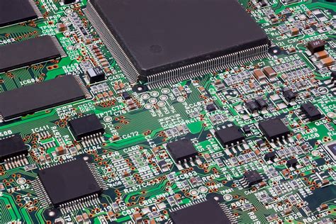
Modern electronics demand PCB manufacturing processes that balance innovation with reliability. When designing advanced circuit boards, you’ll encounter challenges like minimizing signal loss and maximizing thermal efficiency. Leading PCB manufacturing companies now leverage high-density interconnect (HDI) technology to embed components within layers, reducing footprint while boosting performance. This approach not only addresses PCB manufacturing cost concerns but also supports compact, high-speed devices.
Tip: To optimize designs, prioritize collaboration with suppliers early in the prototyping phase. This ensures material choices align with both technical requirements and budget constraints.
Emerging tools like AI-driven simulation software help predict thermal stress and signal integrity issues before production, slashing iteration cycles. For instance, embedded passives eliminate discrete components, streamlining assembly and cutting PCB manufacturing business overhead. However, balancing these advancements with scalability remains critical—especially when integrating flex-circuit hybrids or ultra-thin substrates.
Transitioning to advanced designs requires reevaluating traditional workflows. By adopting modular architectures, you can future-proof systems against rapid technological shifts. For deeper insights into material selection, explore this guide on hybrid PCB materials. Whether refining existing layouts or pioneering new form factors, innovation hinges on harmonizing precision engineering with cost-effective PCB manufacturing strategies.
Rapid Prototyping for Electronics Development
When accelerating electronics development, PCB manufacturing processes must balance speed with precision. Modern PCB manufacturing companies leverage advanced prototyping tools like laser direct imaging (LDI) and automated optical inspection (AOI) to shrink turnaround times from weeks to days. This agility lets you test multiple design iterations faster, reducing time-to-market risks while maintaining quality benchmarks.
A key advantage lies in optimizing PCB manufacturing cost through scalable prototyping. For example, hybrid workflows combine additive manufacturing for low-volume boards with traditional etching for high-volume production. Consider this comparison:
| Prototyping Method | Typical Lead Time | Cost per Unit |
|---|---|---|
| Traditional Etching | 10–14 days | $8–$12 |
| Additive Manufacturing | 2–3 days | $15–$20 |
| Hybrid Approach | 4–5 days | $10–$14 |
By partnering with a PCB manufacturing business specializing in rapid prototyping, you gain access to real-time design feedback and material libraries tailored for high-frequency or flexible circuits. This collaborative approach ensures functional prototypes align with final production specs, avoiding costly mid-stream redesigns. As demand grows for smaller, denser electronics, the ability to iterate quickly becomes a strategic differentiator—whether you’re refining IoT sensors or aerospace-grade systems.
Flex-Circuit Technology Advancements Explained
Modern PCB manufacturing now leverages flex-circuit innovations to meet demands for lightweight, durable electronics. Unlike rigid boards, flexible circuits use polyimide substrates that bend and fold, enabling sleeker designs for wearables, medical devices, and aerospace systems. Leading PCB manufacturing companies prioritize these advancements to reduce PCB manufacturing cost through streamlined processes like roll-to-roll production, which minimizes material waste.
You’ll notice that high-density interconnects (HDIs) and embedded components are becoming standard in flexible designs, allowing for faster signal transmission and improved thermal management. This shift isn’t just technical—it reshapes the PCB manufacturing business by opening markets where space and reliability are non-negotiable. For instance, foldable smartphones or implantable medical tools rely on flex circuits to function under repeated stress.
However, balancing flexibility with durability requires precise material selection and advanced etching techniques. By adopting laser-direct imaging (LDI) and automated optical inspection, manufacturers ensure tighter tolerances while maintaining scalability. These innovations highlight how flex-circuit technology isn’t just an engineering feat—it’s redefining what’s possible in next-gen electronics.
Precision Engineering in Modern PCB Manufacturing
When you examine how cutting-edge electronics achieve their reliability, PCB manufacturing processes stand out as the backbone of precision. Modern PCB manufacturing companies leverage laser direct imaging (LDI) and automated optical inspection (AOI) systems to achieve micrometer-level accuracy in trace routing and layer alignment. These technologies minimize defects while accommodating designs with high-density interconnects—critical for wearables, IoT devices, and AI hardware.
However, balancing PCB manufacturing cost with performance demands strategic material selection. Advanced substrates like polyimide-flex hybrids or low-loss PTFE reduce signal distortion but require specialized handling. This precision-driven approach ensures thermal management and impedance control, directly impacting product longevity in harsh environments.
For businesses scaling their PCB manufacturing business, investing in precision engineering isn’t optional—it’s a competitive necessity. Tight tolerances enable faster prototyping cycles and reduce rework, ultimately accelerating time-to-market. Whether you’re optimizing for aerospace-grade reliability or consumer electronics miniaturization, the marriage of advanced machinery and process rigor defines success in today’s electronics landscape.
Next-Gen Electronics Breakthroughs and Trends
As you push the boundaries of modern electronics, PCB manufacturing innovations are reshaping how devices evolve. Cutting-edge materials like liquid crystal polymer (LCP) and low-loss substrates now enable higher-frequency performance in 5G and IoT systems, while embedded components reduce reliance on bulky connectors. Leading PCB manufacturing companies are leveraging additive printing techniques to create ultra-thin, flexible circuits that fold into wearables or conform to medical implants—advances unthinkable a decade ago.
The drive to optimize PCB manufacturing cost has accelerated automated optical inspection (AOI) systems and AI-powered defect detection, slashing error rates by over 40% in high-volume production. Meanwhile, hybrid designs combining rigid and flex circuits allow engineers to consolidate multiple boards into single assemblies, trimming material waste and assembly time. For R&D teams, balancing performance with PCB manufacturing business realities means prioritizing high-density interconnect (HDI) layouts that maximize functionality without inflating layer counts.
This evolution isn’t just about smaller or faster boards—it’s about reimagining electronics architectures to support quantum computing, autonomous vehicles, and energy-efficient AI processors. As you develop next-gen devices, understanding these synergies between advanced materials, precision engineering, and scalable production will define your competitive edge.
Offshore vs Domestic PCB Production Analysis
When weighing PCB manufacturing options, you’re likely balancing cost efficiency against control and agility. Offshore PCB manufacturing companies often advertise lower PCB manufacturing cost due to reduced labor rates and scaled facilities, but hidden expenses like tariffs, shipping delays, or communication gaps can erode initial savings. Domestic producers, while typically higher in upfront pricing, offer tighter quality oversight and faster iteration cycles—critical for prototyping or compliance-heavy industries.
Your choice hinges on project priorities: offshore might suit high-volume, standardized orders, while domestic PCB manufacturing business models excel in rapid design adjustments and IP security. For R&D-driven projects, shorter supply chains mean you can troubleshoot designs in days rather than weeks. However, global suppliers are closing this gap with localized hubs, blending cost advantages with regional support.
Ultimately, the strategic value of proximity—whether for speed, collaboration, or risk mitigation—often outweighs pure per-unit savings in innovation-centric fields. By mapping your technical requirements and timelines against these trade-offs, you’ll align your PCB manufacturing strategy with broader product goals.
Optimizing Turnaround Times for R&D Projects
When accelerating PCB manufacturing timelines for R&D projects, balancing speed with precision becomes critical. Lean prototyping workflows and strategic partnerships with PCB manufacturing companies can reduce bottlenecks, particularly during iterative design phases. By integrating automated design-for-manufacturability (DFM) tools, you minimize revisions and avoid costly delays—a key factor in managing PCB manufacturing cost while maintaining quality.
Selecting vendors with agile production capabilities ensures faster material sourcing and fabrication. For instance, domestic PCB manufacturing business operations often provide shorter lead times compared to offshore alternatives, though hybrid models (combining local prototyping with scaled offshore production) are gaining traction. Real-time collaboration platforms further streamline communication, allowing engineers to address tolerances or material mismatches before fabrication begins.
To optimize timelines, prioritize modular designs that align with standardized PCB manufacturing processes. This reduces dependency on custom tooling and accelerates testing cycles. Additionally, leveraging data-driven analytics from past projects helps predict potential hurdles, such as thermal management issues or signal integrity challenges, enabling proactive adjustments. By aligning R&D goals with manufacturing realities, you ensure that breakthroughs transition from concept to market-ready solutions without compromising on performance or scalability.
Conclusion
As we’ve seen, the evolution of PCB manufacturing hinges on balancing precision with scalability. Whether you’re evaluating PCB manufacturing companies for prototyping or mass production, understanding the interplay between PCB manufacturing cost and quality becomes critical. Innovations in materials and automation are reshaping the PCB manufacturing business, enabling faster iterations while maintaining reliability.
Your choice between offshore and domestic suppliers impacts not just timelines but also the ability to adapt to design changes mid-project. By prioritizing partnerships with manufacturers that offer transparent cost structures and agile workflows, you position your R&D efforts to capitalize on emerging trends—from ultra-compact wearables to AI-driven systems.
Ultimately, the future of electronics relies on harmonizing cutting-edge engineering with sustainable practices. As demands for smaller, faster, and more efficient devices grow, so too will the strategic importance of optimizing every layer of the PCB manufacturing process.

Frequently Asked Questions
How does PCB manufacturing affect product development timelines?
Modern PCB manufacturing companies leverage automated processes and rapid prototyping to compress R&D cycles. You’ll find that optimized production workflows can reduce lead times by 30-50% compared to traditional methods, critical for iterative design phases.
What drives PCB manufacturing cost variations between projects?
Material selection, layer counts, and flex-circuit integration significantly influence expenses. For instance, high-frequency substrates or embedded components in PCB manufacturing may increase costs by 15-25%, while bulk orders often reduce per-unit pricing through economies of scale.
Should you prioritize domestic or offshore PCB manufacturing business partners?
This depends on your balance of speed versus budget. Domestic providers typically offer faster turnaround for prototyping, whereas offshore PCB manufacturing excels in high-volume production. You’ll want to audit suppliers for certifications like ISO 9001 to ensure quality parity.
Can PCB manufacturing companies support mixed-technology boards?
Leading firms now combine rigid-flex designs, HDI (High-Density Interconnect), and thermal management solutions in single assemblies. Verify if your vendor’s capabilities align with your project’s complexity—especially for aerospace or medical devices requiring MIL-SPEC compliance.
Ready to Start Your PCB Project?
Click here to explore professional PCB manufacturing services tailored for advanced electronics. Whether optimizing prototyping speed or scaling production, you’ll find solutions matching your technical and budgetary needs.