Precision-Driven PCB Manufacturing for Modern Electronics
Key Takeaways
When selecting PCB manufacturing partners for your electronic projects, understanding core competencies separates industry leaders from standard providers. Top-tier PCB manufacturing companies leverage automated optical inspection and 3D laser scoring to ensure micron-level accuracy—critical for high-density interconnect (HDI) designs.
"Always verify certifications like ISO 9001 and IPC Class 3 compliance—these benchmarks directly correlate with defect rates below 0.01% in mission-critical applications."
PCB manufacturing cost optimization requires balancing technical specifications with production scalability. For example:
| Service Tier | Key Consideration | Typical Cost Range |
|---|---|---|
| Prototyping | Layer count & material | $250 – $1,200 |
| High-Volume | Panel utilization rate | $0.02 – $0.15/sq. in |
| Rigid-Flex | Stackup complexity | 30-50% premium |
In the PCB manufacturing business, prioritizing iterative testing protocols reduces time-to-market while maintaining signal integrity. Offshore partnerships can lower expenses by 20-40%, but ensure vendors adhere to ITAR or NIST standards for defense or aerospace projects.
For R&D teams, quick-turn services (72-hour delivery) accelerate validation cycles without compromising impedance control tolerances (±5%). Always request failure analysis reports—this transparency reveals a manufacturer’s capability to support high-reliability applications across thermal, mechanical, and electrical stress thresholds.

Advanced PCB Manufacturing Solutions for Modern Electronics
When developing cutting-edge electronics, choosing the right PCB manufacturing partner determines how effectively you balance innovation, reliability, and PCB manufacturing cost. Modern devices demand high-density layouts, impedance-controlled traces, and materials capable of handling GHz-level frequencies—requirements that push PCB manufacturing companies to refine their fabrication processes. By leveraging automated optical inspection (AOI) and advanced laser drilling, these partners ensure micron-level accuracy for complex designs, whether you’re prototyping IoT sensors or scaling production for aerospace systems.
For businesses optimizing their PCB manufacturing business strategy, offshore partnerships offer cost efficiencies without sacrificing quality. Global supply chain integration enables access to specialized materials like Rogers substrates or polyimide flex layers while maintaining compliance with ITAR or ISO standards. However, balancing speed and precision remains critical: quick-turn services accelerate R&D cycles, but rigorous testing protocols—such as thermal cycling or cross-sectional analysis—safeguard performance in mission-critical applications.
Ultimately, succeeding in today’s market hinges on aligning your project’s technical demands with a manufacturer’s expertise in mixed-signal layouts or high-frequency RF designs. Whether prioritizing rapid prototyping or high-volume production, the right approach to PCB manufacturing ensures your electronics meet both functional benchmarks and long-term reliability goals.
Accelerating R&D With Quick-Turn Prototype Services
In fast-paced electronics development, PCB manufacturing timelines often dictate project viability. Quick-turn prototype services enable you to compress design cycles from weeks to days, allowing iterative testing without derailing R&D schedules. Leading PCB manufacturing companies leverage automated workflows and advanced fabrication techniques to deliver functional prototypes in as few as 24–48 hours, ensuring design flaws are identified before full-scale production.
This approach allows engineers to validate high-frequency signal integrity, thermal management, and material compatibility early in the process. By optimizing PCB manufacturing cost through scalable prototyping, you avoid costly redesigns post-production. For startups and enterprises alike, balancing speed and precision becomes critical when launching next-gen devices—whether IoT sensors or aerospace subsystems.
When selecting PCB manufacturing companies for prototyping, evaluate their capacity to handle complex layer stacks (up to 32 layers) and microvia drilling (<100µm). Advanced providers combine laser direct imaging and automated optical inspection (AOI) to maintain tolerances within ±0.002", ensuring prototypes mirror final-product performance.
The agility of modern PCB manufacturing business models transforms how you approach innovation. By integrating rapid prototyping into your development pipeline, you reduce time-to-market risks while maintaining compliance with evolving industry standards—a strategic advantage in competitive electronics markets.
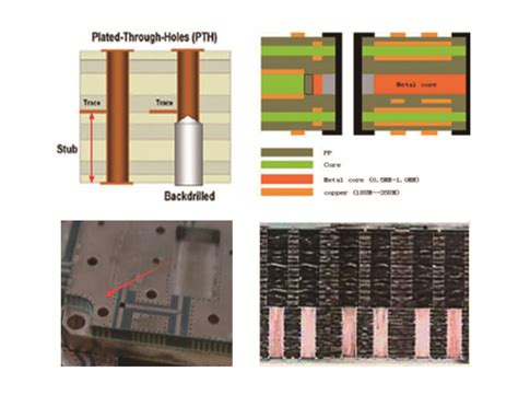
Rigid-Flex Circuit Innovations in Precision PCB Fabrication
When designing modern electronics, you need solutions that balance durability, space efficiency, and signal integrity. PCB manufacturing companies are addressing these demands through rigid-flex circuit innovations, which combine rigid and flexible substrates into a single, seamless design. This hybrid approach eliminates connectors and solder joints, reducing points of failure while enabling complex geometries for wearables, medical devices, and aerospace systems.
By integrating advanced material science and laser-drilled microvias, these circuits achieve high-density interconnects without compromising reliability. However, PCB manufacturing cost considerations remain critical. While rigid-flex designs may initially appear costlier than traditional boards, their ability to consolidate multiple PCBs into one unit often lowers assembly expenses and long-term maintenance. To optimize value, work with providers that specialize in PCB manufacturing business models prioritizing scalability—such as automated optical inspection (AOI) and controlled impedance testing—to ensure consistency across high-volume runs.
For industries requiring lightweight, vibration-resistant solutions, rigid-flex technology exemplifies how PCB manufacturing evolves to meet precision requirements. Its adoption underscores the importance of partnering with fabricators who understand both the technical nuances of flex materials and the economic realities of producing cutting-edge electronics at scale.
ITAR-Compliant Production for High-Reliability Applications
When selecting PCB manufacturing companies for defense or aerospace projects, compliance with International Traffic in Arms Regulations (ITAR) isn’t optional—it’s a non-negotiable requirement. High-reliability applications demand stringent controls over design data, material sourcing, and production processes to prevent unauthorized access to sensitive technologies. Leading PCB manufacturing providers address this by maintaining ITAR-registered facilities, ensuring all personnel and systems adhere to strict security protocols.
Balancing PCB manufacturing cost with compliance can be challenging, but specialized vendors streamline this through controlled environments that minimize risks of data breaches or component tampering. For instance, ITAR-compliant workflows include encrypted design transfers, audited supply chains, and documentation trails for every production batch. These measures not only safeguard intellectual property but also align with MIL-spec standards for durability in extreme conditions.
For businesses in regulated industries, partnering with a PCB manufacturing business that prioritizes ITAR compliance ensures seamless scalability from prototyping to full-scale production. Such partnerships mitigate legal risks while guaranteeing traceability—a critical factor when manufacturing boards for satellite systems, military communications, or medical devices. By integrating compliance into their core operations, trusted manufacturers enable you to focus on innovation without compromising security or performance.

Four Decades of Expertise in Advanced PCB Design
When navigating the complexities of PCB manufacturing, partnering with experienced PCB manufacturing companies ensures your designs meet the rigorous demands of modern electronics. Over four decades, industry leaders have refined methodologies to address evolving challenges—from optimizing PCB manufacturing cost structures to integrating cutting-edge materials for high-frequency applications. This accumulated knowledge allows them to balance precision with scalability, whether you’re prototyping IoT devices or scaling production for aerospace systems.
A seasoned PCB manufacturing business leverages historical data to anticipate thermal management issues, signal integrity constraints, and layer stackup optimization. For instance, rigid-flex circuit fabrication now benefits from decades of material science advancements, reducing failure rates in high-vibration environments. Similarly, advancements in laser-drilled microvias—pioneered through years of R&D—enable denser interconnects without compromising reliability.
When selecting PCB manufacturing companies, their longevity often correlates with robust quality control frameworks. These firms have witnessed industry shifts, from through-hole to surface-mount technology, and adapted processes to maintain compliance with standards like IPC-6012. Their expertise also translates into cost efficiencies; by minimizing material waste and streamlining DFM (Design for Manufacturability) feedback loops, they help lower PCB manufacturing cost while ensuring performance benchmarks are met.
In high-reliability sectors, this institutional knowledge becomes critical. Decades of refining ITAR-compliant workflows and mil-spec certifications mean your projects benefit from proven protocols, reducing time-to-market for mission-critical systems. Whether you’re developing medical devices or defense electronics, partnering with established experts ensures your designs are built on a foundation of tested innovation.
Meeting Demands of High-Precision Electronic Devices
When designing cutting-edge electronics, achieving micron-level accuracy is non-negotiable. PCB manufacturing processes must adapt to handle intricate designs, ultra-fine traces, and tolerances below 0.1mm to meet the exacting standards of medical implants, aerospace systems, and IoT sensors. Leading PCB manufacturing companies leverage laser direct imaging (LDI) and automated optical inspection (AOI) to minimize defects while maintaining scalability.
Balancing PCB manufacturing cost with precision requires strategic material selection—high-frequency laminates or low-loss substrates—paired with advanced plating techniques like ENIG (Electroless Nickel Immersion Gold). For businesses, optimizing PCB manufacturing business workflows—such as integrating DFM (Design for Manufacturability) checks—reduces iterative delays, ensuring prototypes align with functional requirements.
Transitioning from concept to production demands collaboration. By aligning with partners specializing in high-density interconnects (HDI) or embedded passives, you ensure your designs withstand thermal stress and signal integrity challenges. This synergy between innovation and precision not only accelerates time-to-market but future-proofs your electronics in an era where miniaturization and reliability define success.
Optimizing Electronics With Precision PCB Fabrication
Achieving peak performance in modern electronics demands more than standard circuit boards—it requires PCB manufacturing processes engineered for microscopic accuracy. When tolerances shrink to sub-0.1mm scales and signal integrity becomes non-negotiable, partnering with PCB manufacturing companies that prioritize precision ensures your designs translate flawlessly from concept to production.
This optimization begins with advanced fabrication techniques like laser direct imaging (LDI) and automated optical inspection (AOI), which eliminate human error while maintaining tight control over PCB manufacturing cost. For high-density interconnect (HDI) designs or applications requiring impedance control, these methods ensure consistent layer alignment and trace integrity—critical for 5G devices, medical equipment, or aerospace systems.
Balancing performance with affordability remains a key challenge in the PCB manufacturing business, particularly when scaling prototypes to mass production. Leading providers address this by combining design-for-manufacturability (DFM) feedback with material optimization, reducing waste and rework. Whether you’re refining rigid-flex layouts or integrating embedded components, precision-driven workflows enable faster iteration cycles without compromising reliability.
Ultimately, optimizing electronics hinges on aligning your project’s technical demands with a manufacturer’s capability to execute micron-level accuracy—proving that advanced PCB manufacturing isn’t just about building boards but engineering solutions that elevate your product’s functionality.
Global Partnerships for Cost-Effective Offshore Manufacturing
When your PCB manufacturing business requires scaling without compromising quality, strategic global partnerships become essential. By collaborating with certified offshore PCB manufacturing companies, you gain access to specialized expertise and infrastructure that reduces PCB manufacturing cost while maintaining precision. These alliances leverage economies of scale, advanced automation, and region-specific advantages—such as competitive labor markets or material sourcing—to deliver high-performance boards at optimized pricing.
However, cost efficiency doesn’t mean sacrificing reliability. Reputable partners align with ITAR-compliant standards and adhere to rigorous quality controls, ensuring your designs meet exacting specifications even in offshore facilities. This approach is particularly valuable for complex projects like high-density interconnect (HDI) boards or rigid-flex circuits, where technical proficiency directly impacts outcomes.
Through these partnerships, you also mitigate risks like supply chain disruptions by diversifying production hubs. Whether prototyping or transitioning to mass production, a global network enables faster turnaround times and adaptive resource allocation. For businesses balancing tight budgets with the demands of PCB manufacturing, offshore collaboration offers a scalable pathway to innovation without compromising on the precision required for modern electronics.
Conclusion
When navigating the complexities of modern electronics, partnering with the right PCB manufacturing companies ensures your projects meet exacting standards. Precision-driven processes not only enhance performance but also address critical factors like PCB manufacturing cost and scalability. By leveraging expertise in advanced fabrication techniques—from rigid-flex circuit integration to ITAR-compliant production—you secure reliability in high-stakes applications.
For businesses balancing innovation and budgetary constraints, optimizing PCB manufacturing workflows becomes pivotal. Offshore partnerships, when managed strategically, can streamline PCB manufacturing business operations without compromising quality. Whether prototyping or scaling production, aligning with specialists who prioritize high-reliability outcomes ensures your electronics stay ahead in competitive markets. The right approach transforms technical challenges into opportunities, delivering solutions that resonate with both today’s demands and tomorrow’s advancements.
FAQs
How do PCB manufacturing costs affect project budgeting?
Understanding cost drivers like material selection, layer count, and turnaround time helps optimize budgets. High-mix, low-volume projects often prioritize speed, while mass production focuses on economies of scale.
What differentiates top-tier PCB manufacturing companies?
Leading providers combine 40+ years of expertise with certifications like ITAR compliance and ISO 9001. Look for capabilities in rigid-flex circuits and high-reliability applications to ensure performance in demanding environments.
Can PCB manufacturing support rapid prototyping?
Yes. Many partners offer 24-48 hour turnaround for prototypes, accelerating R&D cycles. This agility is critical for testing designs before scaling production.
Is starting a PCB manufacturing business viable today?
While competitive, niche markets like aerospace or medical devices create opportunities. Partnering with offshore fabrication hubs can reduce overhead while maintaining quality.
Ready to Optimize Your PCB Workflow?
For tailored solutions in PCB manufacturing, please click here to explore services that align with your technical and budgetary requirements.