Silkscreen PCB: An Essential Component in Modern Electronics
Introduction
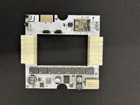
Printed Circuit Boards (PCBs) are the backbone of modern electronics, serving as the foundation upon which electronic components are mounted and interconnected. Among the various layers and features that make up a PCB, the silkscreen layer is one of the most visually distinctive and functionally important. Silkscreen PCB refers to the layer of ink traces printed on the surface of a PCB, typically used to label components, indicate polarity, and provide other critical information. This article delves into the significance of silkscreen in PCB design, its manufacturing process, and its role in ensuring the reliability and usability of electronic devices.
The Role of Silkscreen in PCB Design
The silkscreen layer, often referred to as the “legend” or “component identification layer,” plays a crucial role in the assembly, testing, and maintenance of PCBs. Its primary functions include:
- Component Labeling: Silkscreen is used to label components with their reference designators (e.g., R1, C2, U3), which correspond to the schematic diagram. This labeling is essential for assembly technicians to correctly place and solder components onto the board.
- Polarity and Orientation Indicators: Many electronic components, such as diodes, capacitors, and integrated circuits, have specific polarity or orientation requirements. Silkscreen markings, such as “+” and “-” signs or pin 1 indicators, help ensure that components are installed correctly.
- Test Points and Debugging Information: Silkscreen can be used to mark test points, which are critical for debugging and testing the PCB during and after assembly. These markings help engineers identify where to probe the board to measure voltages, signals, or other parameters.
- Manufacturer Information: Silkscreen often includes the manufacturer’s logo, part number, revision number, and other identifying information. This is useful for traceability and quality control.
- User Instructions: In some cases, silkscreen may include instructions or warnings for the end-user, such as “Do not touch” or “High voltage.”

Silkscreen Manufacturing Process
The silkscreen layer is typically applied after the solder mask layer but before the final surface finish. The process involves several steps:
- Design and Artwork Preparation: The silkscreen layer is designed using PCB design software, such as Altium Designer, Eagle, or KiCad. The designer creates the text, symbols, and other markings that will be printed on the PCB. The artwork is then exported as a Gerber file, which is used by the PCB manufacturer.
- Screen Printing: The traditional method of applying silkscreen is through screen printing. A fine mesh screen is coated with a photosensitive emulsion, and the silkscreen artwork is transferred onto the screen using a photolithographic process. Ink is then forced through the screen onto the PCB surface using a squeegee. This method is cost-effective and suitable for large-scale production.
- Liquid Photo Imaging (LPI): For higher precision and finer details, Liquid Photo Imaging (LPI) is often used. In this process, a liquid photo-imageable ink is applied to the PCB surface, exposed to UV light through a photomask, and then developed to remove the unexposed areas. LPI offers better resolution and durability compared to traditional screen printing.
- Direct Legend Printing (DLP): Some manufacturers use inkjet or laser printing technologies to apply the silkscreen directly onto the PCB. This method offers high precision and flexibility, allowing for quick changes in the design without the need for new screens or masks.
- Curing: After the ink is applied, it is cured using heat or UV light to ensure it adheres properly to the PCB surface and is resistant to wear and tear.
Challenges and Considerations in Silkscreen PCB Design
While silkscreen is a relatively simple aspect of PCB design, there are several challenges and considerations that designers must keep in mind:
- Legibility: The text and symbols on the silkscreen must be legible, even at small sizes. This requires careful selection of font type, size, and spacing. Typically, a sans-serif font is used for better readability.
- Placement: Silkscreen markings must be placed in such a way that they do not interfere with solder pads, vias, or other critical areas of the PCB. This requires precise alignment and spacing.
- Color Contrast: The color of the silkscreen ink should contrast well with the solder mask color to ensure visibility. White is the most common silkscreen color, but other colors like yellow or black may be used depending on the solder mask color.
- Durability: The silkscreen ink must be durable enough to withstand the rigors of PCB assembly, including exposure to high temperatures during soldering and cleaning processes. It should also resist fading, scratching, and chemical exposure over the life of the product.
- Compliance with Standards: Silkscreen design must comply with industry standards, such as IPC-7351, which provides guidelines for component labeling, polarity markings, and other aspects of PCB design.
Advancements in Silkscreen Technology
As PCB technology continues to evolve, so does the technology used for silkscreen application. Some of the recent advancements include:
- High-Resolution Inkjet Printing: Modern inkjet printers offer high-resolution printing capabilities, allowing for finer details and more complex designs on the silkscreen layer. This is particularly useful for high-density PCBs with small components.
- 3D Silkscreen Printing: Some manufacturers are experimenting with 3D printing technologies to create raised or embossed silkscreen markings. This can improve tactile feedback and visibility, especially in low-light conditions.
- Environmentally Friendly Inks: With increasing emphasis on sustainability, there is a growing demand for eco-friendly silkscreen inks that are free from harmful chemicals and solvents.
- Automated Inspection: Automated optical inspection (AOI) systems are now capable of inspecting the silkscreen layer for defects such as smudging, misalignment, or missing markings. This helps ensure the quality and reliability of the PCB.
Conclusion
Silkscreen PCB is an essential component in modern electronics, providing critical information for assembly, testing, and maintenance. While it may seem like a minor detail in the grand scheme of PCB design, the silkscreen layer plays a vital role in ensuring the functionality, reliability, and usability of electronic devices. As technology continues to advance, we can expect further innovations in silkscreen application methods, materials, and design techniques, further enhancing the capabilities of PCBs in the ever-evolving world of electronics.