PCB Inductors: Design, Applications, and Future Trends
Introduction
Printed Circuit Board (PCB) inductors are integral components in modern electronics, playing a crucial role in a wide range of applications, from power supplies to RF circuits. As the demand for miniaturization and integration in electronic devices continues to grow, PCB inductors have become increasingly important due to their ability to be directly fabricated onto the PCB, saving space and reducing assembly complexity. This article explores the design principles, applications, and future trends of PCB inductors, providing a comprehensive overview of this essential component.
1. Fundamentals of PCB Inductors
1.1 What is a PCB Inductor?
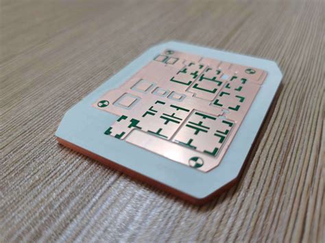
A PCB inductor is an inductor that is fabricated directly onto a printed circuit board. Unlike traditional wire-wound inductors, which are discrete components, PCB inductors are formed using the conductive traces on the PCB itself. These inductors can be designed in various shapes and sizes, depending on the specific requirements of the circuit.
1.2 Basic Principles of Inductance
Inductance is a property of an electrical conductor that opposes changes in current. It is defined by the relationship between the voltage across the inductor and the rate of change of current through it. The inductance (L) of a coil is given by:
[ L = \frac{N^2 \mu A}{l} ]
where:
- ( N ) is the number of turns,
- ( \mu ) is the permeability of the core material,
- ( A ) is the cross-sectional area of the coil,
- ( l ) is the length of the coil.
In the case of PCB inductors, the “coil” is formed by the conductive traces on the PCB, and the core material is often the PCB substrate itself or an additional magnetic material layer.
1.3 Types of PCB Inductors
PCB inductors can be categorized based on their structure and application:
- Spiral Inductors: These are the most common type of PCB inductors, consisting of a spiral trace on the PCB. They are widely used in RF and microwave circuits.
- Meander Inductors: These inductors have a meandering trace pattern and are used in applications where space is limited.
- Planar Transformers: These are more complex structures that combine multiple inductors to form a transformer directly on the PCB.
- Embedded Inductors: These inductors are embedded within the layers of the PCB, allowing for higher inductance values and better integration.

2. Design Considerations for PCB Inductors
2.1 Trace Geometry
The geometry of the conductive trace is a critical factor in determining the inductance of a PCB inductor. Key parameters include:
- Trace Width: Wider traces reduce resistance but may limit the number of turns that can fit in a given area.
- Trace Spacing: Closer spacing increases the inductance but can also increase parasitic capacitance.
- Number of Turns: More turns generally increase inductance but also increase resistance and parasitic capacitance.
2.2 Substrate Material
The substrate material of the PCB affects the inductance and performance of the inductor. Common substrate materials include:
- FR-4: A standard PCB material with moderate dielectric properties. It is widely used but has limitations in high-frequency applications.
- Rogers Material: A high-frequency substrate material with better dielectric properties, suitable for RF and microwave applications.
- Ferrite Layers: Adding ferrite layers to the PCB can increase the inductance by enhancing the magnetic flux.
2.3 Parasitic Effects
PCB inductors are subject to various parasitic effects that can impact their performance:
- Parasitic Capacitance: The capacitance between the turns of the inductor can affect the resonant frequency and overall performance.
- Parasitic Resistance: The resistance of the conductive traces can lead to power losses and reduced Q-factor.
- Skin Effect: At high frequencies, current tends to flow on the surface of the conductor, increasing effective resistance.
2.4 Thermal Considerations
Inductors generate heat due to resistive losses, and in PCB inductors, this heat must be managed to prevent damage to the PCB and surrounding components. Proper thermal management techniques, such as thermal vias and heat sinks, are essential in high-power applications.
3. Applications of PCB Inductors
3.1 Power Electronics
PCB inductors are widely used in power electronics, including:
- DC-DC Converters: Inductors are essential components in buck, boost, and buck-boost converters, where they store and transfer energy.
- Voltage Regulators: Inductors are used in switching regulators to smooth out voltage fluctuations.
- Power Filters: Inductors are used in conjunction with capacitors to filter out noise and ripple in power supplies.
3.2 RF and Microwave Circuits
In RF and microwave circuits, PCB inductors are used for:
- Impedance Matching: Inductors are used to match the impedance of different circuit stages, ensuring maximum power transfer.
- Filters: Inductors are key components in low-pass, high-pass, and band-pass filters.
- Oscillators: Inductors are used in LC oscillators to generate stable frequencies.
3.3 Communication Systems
PCB inductors play a vital role in communication systems, including:
- Antennas: Inductors are used in antenna matching networks to optimize performance.
- RF Amplifiers: Inductors are used in RF amplifiers for biasing and impedance matching.
- Signal Processing: Inductors are used in various signal processing applications, such as demodulation and modulation.
3.4 Automotive Electronics
In automotive electronics, PCB inductors are used in:
- Engine Control Units (ECUs): Inductors are used in power supply circuits and signal filtering.
- Infotainment Systems: Inductors are used in audio amplifiers and RF circuits.
- Advanced Driver-Assistance Systems (ADAS): Inductors are used in radar and sensor systems.
4. Advantages and Challenges of PCB Inductors
4.1 Advantages
- Miniaturization: PCB inductors allow for significant space savings compared to traditional inductors.
- Integration: They can be directly integrated into the PCB, reducing assembly complexity and cost.
- Customization: PCB inductors can be designed to meet specific inductance and performance requirements.
- High-Frequency Performance: PCB inductors can be optimized for high-frequency applications, making them suitable for RF and microwave circuits.
4.2 Challenges
- Limited Inductance: PCB inductors typically have lower inductance values compared to traditional wire-wound inductors.
- Parasitic Effects: Parasitic capacitance and resistance can limit the performance of PCB inductors, especially at high frequencies.
- Thermal Management: Managing heat dissipation in PCB inductors can be challenging, particularly in high-power applications.
- Manufacturing Complexity: Designing and manufacturing PCB inductors requires specialized knowledge and equipment.

5. Future Trends in PCB Inductors
5.1 Advanced Materials
The development of new materials, such as high-permeability substrates and low-loss dielectrics, is expected to enhance the performance of PCB inductors. These materials can increase inductance, reduce losses, and improve thermal management.
5.2 3D Printing
3D printing technology is being explored as a method for fabricating PCB inductors with complex geometries. This approach could enable the creation of inductors with higher inductance values and better performance in a smaller footprint.
5.3 Integration with Active Components
Future trends may see the integration of PCB inductors with active components, such as transistors and diodes, to create more compact and efficient circuits. This integration could lead to the development of new types of integrated circuits (ICs) that combine passive and active elements.
5.4 AI-Driven Design
Artificial intelligence (AI) and machine learning (ML) are being used to optimize the design of PCB inductors. AI-driven design tools can analyze vast amounts of data to identify the best geometries, materials, and configurations for specific applications, leading to more efficient and high-performance inductors.
5.5 Flexible and Stretchable PCBs
The development of flexible and stretchable PCBs is opening up new possibilities for PCB inductors. These inductors could be used in wearable electronics, flexible displays, and other applications where traditional rigid PCBs are not suitable.
Conclusion
PCB inductors are essential components in modern electronics, offering significant advantages in terms of miniaturization, integration, and customization. While they present certain challenges, ongoing advancements in materials, manufacturing techniques, and design tools are expected to overcome these limitations and further enhance their performance. As the demand for smaller, more efficient electronic devices continues to grow, PCB inductors will play an increasingly important role in shaping the future of electronics.
