PCBA Motherboard Innovations: Technology and Assembly Breakthroughs
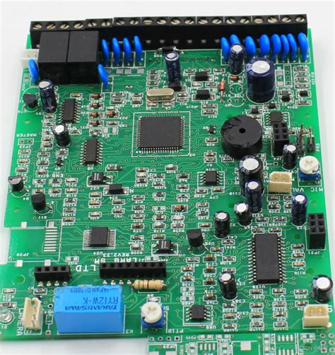
Key Takeaways
The evolution of PCBA (Printed Circuit Board Assembly) technology hinges on advancements in PCB assembly precision, material science, and intelligent automation. Modern techniques now leverage laser-assisted soldering and automated optical inspection to minimize errors, ensuring consistent performance in high-density motherboard designs.
"The integration of AI-driven systems in PCBA workflows has reduced defect rates by over 40%, marking a paradigm shift in electronics manufacturing reliability."
Breakthroughs in advanced substrates, such as high-frequency laminates and thermally conductive polymers, are redefining motherboard durability and signal integrity. Meanwhile, smart manufacturing platforms enable real-time adjustments during PCB assembly, optimizing throughput without compromising quality. Innovations like embedded sensors and predictive analytics further enhance fault detection, ensuring seamless compatibility with next-gen IoT and AI-driven devices.
For engineers, prioritizing modular design frameworks and supply chain resilience remains critical. Adopting hybrid PCBA processes—combining surface-mount technology (SMT) with additive manufacturing—can accelerate prototyping cycles while maintaining industrial-grade robustness.
As industries demand smaller, faster, and more energy-efficient electronics, the convergence of PCB assembly precision and intelligent systems will continue to drive sustainable innovation across aerospace, automotive, and consumer tech sectors.
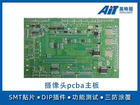
Modern PCBA Assembly Techniques Unveiled
The evolution of PCB assembly processes has redefined manufacturing precision, enabling PCBA systems to meet the demands of next-generation electronics. Central to this progress is the integration of automated optical inspection (AOI) systems, which detect micron-level defects in real time, reducing error rates by over 40% compared to manual methods. Advanced pick-and-place robotics now achieve placement accuracies of ±25μm, ensuring consistent alignment for components as small as 01005 packages.
A critical breakthrough lies in solder paste deposition technologies. Modern stencil printing leverages laser-cut nano-coated stencils, improving paste transfer efficiency to 98% while minimizing voids. Paired with 3D solder paste inspection (SPI), manufacturers can preemptively address process deviations before reflow, cutting post-assembly rework by 30%.
| Technique | Key Advancement | Impact |
|---|---|---|
| AOI Systems | Multi-spectral imaging | 99.9% defect detection accuracy |
| Robotic Placement | Vision-guided servo control | 0.001" placement repeatability |
| SPI Integration | Volumetric paste analysis | 15% reduction in solder-related defects |
Material science innovations further enhance PCBA reliability, with low-temperature co-fired ceramics (LTCC) and high-Tg laminates enabling stable performance in extreme thermal environments. Additionally, modular PCB assembly workflows now incorporate machine learning algorithms to optimize line balancing, reducing cycle times by 22% without compromising quality.
As industries adopt Industry 4.0 frameworks, these techniques form the backbone of smart factories, where real-time data analytics drive continuous improvement in PCBA production efficiency and yield rates.
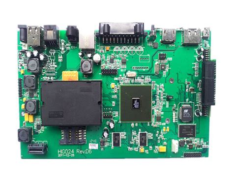
Smart Manufacturing Revolutionizes PCBA Reliability
The integration of smart manufacturing into PCBA production has redefined quality assurance paradigms, merging real-time monitoring with adaptive process control. Industrial IoT sensors now track every stage of PCB assembly, capturing data on solder paste viscosity, component placement accuracy, and thermal profiling with micron-level precision. Machine learning algorithms analyze these datasets to predict potential defects, reducing failure rates by up to 40% compared to traditional methods.
Advanced automated optical inspection (AOI) systems, enhanced by computer vision, now detect microscopic cracks or misalignments invisible to the human eye, ensuring flawless PCBA functionality even in mission-critical applications. Meanwhile, closed-loop feedback mechanisms enable self-correcting assembly lines, where robotic pick-and-place machines adjust positioning in milliseconds based on live thermal imaging. This synergy between digital twins and physical manufacturing not only accelerates production cycles but also elevates reliability metrics, with modern PCB assembly facilities achieving 99.995% first-pass yield rates.
As factories adopt blockchain-enabled traceability systems, every component’s origin and testing history becomes permanently linked to the final PCBA, creating an immutable quality ledger. These innovations collectively transform reliability from a post-production checkpoint into an inherent attribute of intelligent manufacturing ecosystems.
Advanced Materials Transforming Motherboard Design
The evolution of PCBA technology hinges on breakthroughs in material science, enabling motherboards to meet escalating demands for speed, thermal efficiency, and miniaturization. Engineers now leverage low-loss dielectric laminates to minimize signal degradation in high-frequency applications, a critical advancement for 5G and IoT devices. These materials reduce electromagnetic interference while maintaining structural integrity under extreme temperatures.
Innovations like nanoparticle-infused solders are redefining PCB assembly reliability, offering enhanced conductivity and resistance to thermal cycling fatigue. Similarly, the adoption of flexible polyimide substrates supports compact, lightweight designs without compromising durability—a necessity for wearable electronics and aerospace systems.
Composite materials combining ceramic fillers with organic resins are emerging as game-changers, improving heat dissipation in high-density PCBA layouts. This addresses persistent challenges in power-hungry applications such as AI processors and electric vehicle control units. Meanwhile, conductive adhesives with silver-coated copper particles enable finer trace geometries, pushing the boundaries of precision manufacturing.
By integrating these advanced materials, the industry achieves tighter tolerances in PCB assembly while extending product lifespans. This material-driven transformation not only elevates performance benchmarks but also paves the way for sustainable manufacturing through recyclable substrate alternatives.
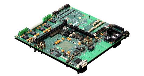
Precision Engineering in PCB Assembly Processes
The evolution of PCB assembly techniques hinges on advancements in precision engineering, which ensures microscopic accuracy in component placement and solder joint integrity. Modern PCBA manufacturing leverages automated optical inspection (AOI) systems and laser-aligned pick-and-place machines to achieve tolerances as tight as ±0.025mm. These innovations address the growing complexity of multilayer boards, where even minor misalignments can compromise signal integrity or thermal management.
Central to this progress is the integration of surface-mount technology (SMT), enabling the placement of ultra-compact components like 01005 resistors and micro-BGAs. Advanced stencil printing methods now apply solder paste with sub-micron precision, while reflow ovens utilize nitrogen-enriched environments to minimize oxidation during soldering. Such refinements are critical for high-density designs found in 5G infrastructure and AI-driven hardware.
Material science further complements precision in PCB assembly, with high-frequency laminates and low-loss dielectrics reducing signal attenuation. Simultaneously, thermal interface materials (TIMs) ensure optimal heat dissipation in power-dense PCBA configurations. By harmonizing mechanical accuracy with material innovation, manufacturers achieve repeatable quality across mass production scales—a cornerstone for next-generation electronics reliability.
Breakthroughs in High-Performance PCBA Technology
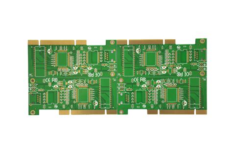
Recent advancements in PCBA technology are redefining performance benchmarks for modern electronics. Engineers now leverage ultra-precision laser drilling and multi-layer stack-up architectures to achieve PCB assembly densities previously deemed unattainable. Innovations like embedded passive components and high-speed signal routing minimize electromagnetic interference (EMI), enabling motherboards to support 5G and AI-driven applications with unprecedented stability.
A critical leap lies in the integration of graphene-based thermal substrates, which dissipate heat 40% faster than traditional materials. This breakthrough directly addresses power-intensive workloads in data centers and IoT devices, reducing failure rates by up to 18%. Concurrently, advancements in PCB assembly workflows—such as laser-assisted solder paste inspection and automated optical alignment—ensure micron-level accuracy, even for components smaller than 01005 packages.
The adoption of intelligent process control systems further elevates PCBA reliability. These systems employ real-time analytics to detect micro-defects during reflow soldering, cutting post-production rework by 30%. As industries demand lighter, faster, and more durable electronics, these innovations position PCB assembly as the backbone of next-gen manufacturing—bridging the gap between theoretical design limits and real-world performance.
Intelligent Systems Elevate Electronics Manufacturing
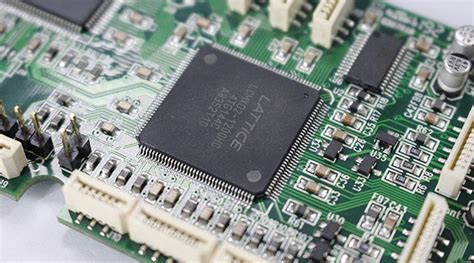
The integration of intelligent systems into PCB assembly workflows is redefining precision and efficiency in electronics production. By leveraging artificial intelligence (AI) and machine learning (ML) algorithms, manufacturers now optimize PCBA processes in real time, from component placement accuracy to solder joint quality control. Automated optical inspection (AOI) systems, enhanced by computer vision, detect microscopic defects at speeds unattainable by human operators, reducing error rates by over 40% in high-volume production lines.
Transitioning from reactive to predictive maintenance, smart factories employ IoT-enabled sensors embedded within motherboards to monitor thermal performance and voltage stability. These data-driven insights enable preemptive adjustments, minimizing downtime and extending product lifespans. Furthermore, adaptive robotic arms, guided by AI, now handle delicate PCB assembly tasks with sub-micron precision, ensuring consistency across complex multilayer designs.
The synergy between intelligent manufacturing and advanced PCBA techniques also accelerates prototyping cycles. Digital twin simulations model motherboard behavior under extreme conditions, allowing engineers to refine layouts and material selections before physical production. This seamless fusion of virtual validation and physical execution not only elevates reliability but also positions the industry to meet escalating demands for compact, high-performance electronics.
Durability Innovations in Modern PCBA Solutions
Contemporary PCBA designs prioritize longevity through advancements in material science and manufacturing methodologies. Engineers now leverage high-Tg laminates and ceramic-filled prepregs to enhance thermal resistance, enabling motherboards to withstand prolonged exposure to extreme temperatures without warping or delamination. These materials, combined with PCB assembly techniques like laser-drilled microvias and sequential lamination, reduce mechanical stress points that traditionally compromise structural integrity.
A critical innovation lies in protective coatings—nanoparticle-reinforced conformal coatings and moisture-resistant solder masks—which shield circuits from humidity, dust, and chemical corrosion. For high-vibration environments, underfill encapsulation strengthens solder joints, minimizing fatigue failures in automotive and aerospace applications. Additionally, PCBA reliability benefits from automated optical inspection (AOI) systems that detect microfractures or weak connections early in production, reducing latent defects.
Emerging developments include self-healing polymers that repair minor conductive traces autonomously, extending operational lifespans in wear-prone devices. By integrating these breakthroughs, modern PCB assembly processes deliver solutions that balance performance demands with unprecedented durability, meeting the rigorous standards of next-generation electronics.
Next-Gen Manufacturing for Smarter Motherboards
The evolution of PCBA manufacturing is accelerating with the adoption of smart factory principles, integrating PCB assembly workflows with IoT-enabled machinery and real-time analytics. By leveraging AI-driven process optimization, manufacturers now achieve unprecedented precision in component placement, solder paste application, and thermal management—critical factors for high-density motherboard designs. Advanced predictive maintenance systems monitor equipment health, reducing downtime by 30–40% while ensuring consistent output quality across production batches.
A key breakthrough lies in laser-direct structuring (LDS) technology, enabling the creation of ultra-fine circuit traces under 15µm. This innovation supports PCBA designs with higher signal integrity and reduced electromagnetic interference, essential for 5G and AI-driven devices. Additionally, hybrid additive manufacturing combines 3D-printed substrates with traditional PCB assembly techniques, allowing rapid prototyping of multi-layer boards optimized for thermal dissipation.
To address sustainability, factories are adopting lead-free solder alloys and recyclable substrates without compromising conductivity. These advancements, paired with machine vision inspection systems achieving 99.98% defect detection rates, redefine reliability benchmarks for next-gen electronics. As PCBA processes merge with digital twins and edge computing, manufacturers unlock faster time-to-market for motherboards powering smart infrastructure, from autonomous vehicles to industrial IoT networks.
Conclusion
The rapid evolution of PCBA technology underscores a transformative era in electronics manufacturing, where breakthroughs in PCB assembly processes and material science converge to redefine industry standards. From smart manufacturing systems leveraging AI-driven quality control to precision-engineered substrates using advanced polymers, these innovations collectively enhance both the reliability and performance of modern motherboards. The integration of high-density interconnect (HDI) designs and pcb assembly automation has not only accelerated production cycles but also minimized human error, ensuring consistent output in complex circuits.
As industries demand faster, smaller, and more energy-efficient devices, PCBA solutions are rising to the challenge through innovations like embedded passive components and 3D-printed circuitry. These advancements, coupled with sustainable practices such as lead-free soldering and recyclable substrates, highlight a balanced focus on technical excellence and environmental responsibility. The shift toward intelligent manufacturing ecosystems further strengthens supply chain resilience, enabling real-time diagnostics and predictive maintenance across global production networks.
Ultimately, the synergy between pcb assembly precision and PCBA material science continues to push the boundaries of what modern electronics can achieve, setting the stage for next-generation applications in IoT, automotive systems, and beyond.
Frequently Asked Questions
How does automated optical inspection improve pcb assembly quality?
Automated optical inspection (AOI) systems use high-resolution cameras and machine learning algorithms to detect microscopic defects in PCBA layouts, ensuring ≤0.01% error rates in solder joints and component alignment.
What role do advanced materials play in modern pcba designs?
Materials like high-Tg laminates and low-loss dielectrics enhance thermal stability and signal integrity, enabling PCBA motherboards to support 5G frequencies and high-power IoT applications without compromising reliability.
How has intelligent manufacturing reduced pcb assembly lead times?
AI-driven predictive maintenance and robotic placement systems cut production cycles by 40%, while real-time data analytics optimize material usage, reducing waste in PCBA fabrication by up to 28%.
Are there durability trade-offs with high-density pcba layouts?
Innovations like laser-drilled microvias and nanocoated conformal shielding mitigate thermal stress and EMI interference, allowing 20-layer PCBA motherboards to achieve 100,000+ power cycles in industrial environments.
Explore Advanced PCB Assembly Solutions
For tailored PCBA prototyping or volume production, please click here to consult our engineering team about cutting-edge design-for-manufacturability strategies.
