Optimizing PCB Sub Assembly for Enhanced Manufacturing Quality
Key Takeaways
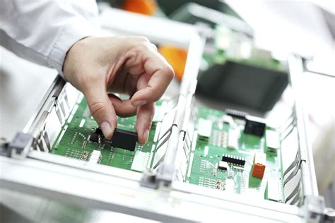
Effective optimization of PCB assembly processes hinges on three core principles: design precision, material integrity, and systematic validation. By prioritizing automated optical inspection (AOI) and X-ray testing during PCBA stages, manufacturers can identify latent defects such as soldering inconsistencies or component misalignments early in production.
Tip: Implement cross-functional collaboration between design and manufacturing teams to align PCB sub-assembly tolerances with end-product performance requirements.
Key steps include adopting surface-mount technology (SMT) for higher component density, optimizing solder paste application through stencil design refinements, and enforcing thermal profiling to prevent board warping during reflow. Rigorous in-circuit testing (ICT) and environmental stress screening (ESS) further ensure reliability under operational conditions.
Transitioning to traceable documentation for every PCBA batch not only streamlines quality audits but also supports continuous improvement by correlating test data with field performance metrics. This approach minimizes rework cycles while reinforcing compliance with industry standards like IPC-A-610.
Precision Engineering in PCB Sub Assembly
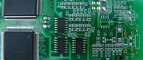
Precision engineering forms the backbone of high-quality PCB assembly, ensuring that sub-assemblies meet exacting performance standards. By integrating advanced PCBA design methodologies, manufacturers minimize tolerance mismatches and signal integrity issues, which are critical in complex electronic systems. Modern techniques leverage automated optical inspection (AOI) and laser-drilled microvias to achieve micron-level accuracy, particularly in multilayer boards.
| Engineering Factor | Traditional Approach | Precision-Driven Solution |
|---|---|---|
| Component Placement | Manual Alignment | Robotic Pick-and-Place Systems |
| Soldering Accuracy | Wave Soldering | Reflow Soldering with Nitrogen Blanket |
| Trace Width Control | ±10% Tolerance | ±2% Laser-Etched Traces |
The shift toward precision-driven PCBA processes reduces electromagnetic interference (EMI) risks and enhances thermal management. For instance, embedded passive components and controlled impedance routing mitigate signal loss in high-frequency applications. Rigorous design for manufacturability (DFM) checks further align sub-assembly workflows with end-product requirements, ensuring seamless integration in final devices. By prioritizing precision at every stage—from schematic validation to final inspection—manufacturers elevate both yield rates and long-term reliability in PCB assembly ecosystems.
Testing Protocols for Reliable PCB Sub Assembly
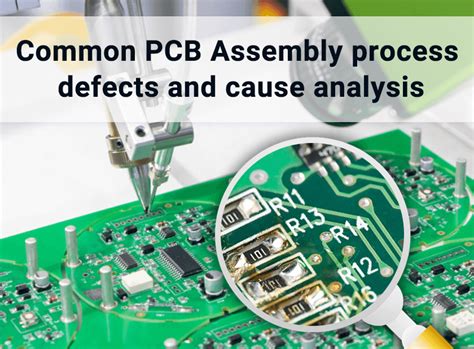
Implementing robust testing protocols is critical to ensuring the long-term reliability of PCB assembly processes. Modern automated optical inspection (AOI) systems scan PCBA components for soldering defects, misalignments, or micro-cracks, achieving accuracy rates exceeding 99.7%. For high-density boards, in-circuit testing (ICT) validates electrical connectivity by measuring resistance, capacitance, and voltage thresholds across circuits. Functional testing then simulates real-world operating conditions, stress-testing components under varying loads and temperatures to identify potential failure points.
To address environmental resilience, thermal cycling tests expose PCB sub assembly units to rapid temperature fluctuations, verifying their stability in extreme climates. Concurrently, vibration testing replicates mechanical stresses encountered during transportation or operation, ensuring solder joints and connectors remain intact. Advanced manufacturers integrate boundary scan testing to diagnose complex integrated circuits, reducing debugging time by up to 40%.
These protocols not only align with ISO 9001 and IPC-A-610 standards but also create a feedback loop for refining design tolerances and material selection. By prioritizing rigorous testing in PCB assembly workflows, manufacturers mitigate risks of field failures while optimizing product lifecycle performance.
Enhancing Product Performance via PCB Optimization
Optimizing PCB assembly processes directly impacts the functional efficiency and longevity of electronic devices. By refining design parameters such as trace routing, component placement, and layer stack-up, engineers can minimize signal interference and thermal stress—critical factors in high-density PCBA applications. For instance, implementing impedance-controlled routing reduces data transmission errors, while strategic placement of heat-generating components enhances thermal dissipation.
Material selection also plays a pivotal role. Utilizing high-performance substrates like FR-4 with low dielectric loss or polyimide for flexible circuits ensures mechanical stability across operating conditions. Advanced soldering alloys and conformal coatings further safeguard against environmental factors, extending the lifecycle of PCB sub-assemblies.
Testing protocols, including automated optical inspection (AOI) and in-circuit testing (ICT), validate design optimizations by identifying latent defects in PCB assembly lines. These methods, combined with simulation tools like finite element analysis (FEA), enable iterative improvements without physical prototyping. Such precision-driven adjustments not only elevate product reliability but also align with lean manufacturing principles, reducing waste and rework in PCBA workflows.
By harmonizing design innovation with rigorous validation, manufacturers achieve measurable gains in performance metrics—from power efficiency to signal integrity—ensuring optimized PCB sub-assemblies meet evolving industry demands.
Streamlining PCB Sub Assembly Manufacturing
Efficient PCB assembly processes form the backbone of high-quality electronics manufacturing, requiring seamless integration of design, component placement, and testing. To optimize operational workflows, manufacturers increasingly adopt automated optical inspection (AOI) systems, which reduce human error while accelerating throughput. By aligning PCBA stages with design for manufacturability (DFM) principles, engineers minimize rework risks by addressing potential issues like component spacing or thermal management early in development.
A critical phase involves refining surface-mount technology (SMT) applications, where precise solder paste deposition and reflow profiling ensure consistent electrical connections. Advanced factories now deploy traceability systems that track each sub-assembly through production, enabling rapid root-cause analysis if defects emerge. For instance, integrating real-time process monitoring with PCB assembly lines allows adjustments to be made mid-production, preventing costly batch failures.
Moreover, lean manufacturing strategies—such as just-in-time inventory management—streamline material flows, reducing lead times without compromising PCBA quality. Collaborative robotics further enhances precision in tasks like micro-component placement, particularly for high-density interconnect (HDI) boards. These innovations, combined with rigorous process standardization, create a scalable framework for maintaining manufacturing reliability across varying production volumes.
Key Steps to Improve PCB Assembly Quality
Achieving consistent quality in PCB assembly requires a systematic approach that integrates precision planning with robust execution. First, thorough design for manufacturability (DFM) analysis ensures component placement aligns with PCBA production capabilities, minimizing errors during soldering or mounting. Engineers must validate material compatibility, particularly for high-frequency or thermal-sensitive applications, to prevent delamination or solder joint failures.
Equally critical is implementing automated optical inspection (AOI) systems at multiple stages to detect flaws like tombstoning or insufficient solder paste deposition. Pairing AOI with in-circuit testing (ICT) verifies electrical functionality, isolating defects before final integration. For PCB assembly involving mixed-technology components, controlled reflow profiles and nitrogen-assisted soldering enhance joint reliability, especially for fine-pitch BGAs or QFNs.
Another vital step involves adopting traceability protocols using barcodes or RFID tags, enabling real-time monitoring of PCBA workflows. This data-driven strategy helps identify process bottlenecks while maintaining compliance with industry standards like IPC-A-610. Finally, post-assembly environmental stress testing—including thermal cycling and vibration simulations—validates long-term durability, ensuring end-products meet rigorous operational demands. By harmonizing these measures, manufacturers can systematically elevate PCB assembly quality while reducing rework rates.
Advanced Techniques for PCB Sub Assembly
Modern PCB assembly processes demand cutting-edge methodologies to address evolving manufacturing challenges. One critical advancement involves automated optical inspection (AOI) systems, which leverage machine vision to detect micro-scale defects in PCBA components, such as solder bridging or misaligned traces. For high-density designs, 3D solder paste inspection (SPI) ensures precise deposition volumes, reducing rework rates by up to 40% compared to manual methods.
Another breakthrough lies in thermo-compressive bonding for multilayer boards, which enhances interlayer conductivity while minimizing thermal stress. Engineers are also adopting predictive maintenance algorithms for pick-and-place machinery, analyzing real-time data to preempt component misplacement or feeder jams.
To optimize signal integrity, impedance-controlled routing techniques are now standard in PCB sub assembly, particularly for high-frequency applications. Pairing this with embedded passive components reduces parasitic effects, improving overall circuit reliability.
Leading manufacturers now implement closed-loop feedback systems that integrate design software with assembly-line analytics, enabling iterative refinements to PCBA workflows. These innovations not only elevate precision but also align with industry shifts toward scalable, IoT-ready production frameworks. By merging advanced automation with data-driven insights, stakeholders achieve tighter tolerances and faster time-to-market—key drivers in today’s competitive electronics landscape.
Boosting Reliability Through Rigorous PCB Testing
Rigorous testing protocols form the backbone of high-quality PCB assembly, ensuring that PCBA products meet stringent performance and durability standards. Modern manufacturing leverages advanced methodologies such as In-Circuit Testing (ICT) and Automated Optical Inspection (AOI) to identify solder joint defects, component misalignments, or electrical inconsistencies. By integrating environmental stress screening—including thermal cycling and vibration testing—engineers can simulate real-world operating conditions, uncovering latent flaws that might compromise long-term reliability.
Transitioning from design to production, Design-for-Testability (DFT) principles streamline validation processes, enabling seamless fault detection during PCB assembly. For instance, boundary scan testing validates complex circuitry in densely packed PCBA units, reducing post-production failures. Additionally, functional testing verifies end-to-end system behavior, ensuring compatibility with application-specific requirements.
To maintain consistency, manufacturers adopt statistical process control (SPC) tools, monitoring key metrics like solder paste viscosity and reflow oven profiles. Pairing these measures with cross-functional collaboration between design and testing teams minimizes rework cycles while accelerating time-to-market. By prioritizing rigorous validation at every stage, organizations not only enhance product lifespan but also fortify their reputation for delivering mission-critical electronics.
PCB Sub Assembly Best Practices for Quality
Implementing PCB assembly best practices begins with meticulous material selection and process validation. Prioritizing high-grade substrates and temperature-resistant components ensures stability during PCBA manufacturing, particularly in high-stress environments. Automated optical inspection (AOI) and X-ray testing should complement manual checks to identify micro-scale defects, such as solder bridging or misaligned traces, before final integration.
Adopting standardized workflows—including controlled soldering profiles and anti-static protocols—reduces variability in PCB sub-assembly stages. For instance, maintaining a nitrogen-rich atmosphere during reflow soldering minimizes oxidation, enhancing joint integrity. Additionally, real-time data logging enables traceability, allowing engineers to correlate process parameters with performance outcomes.
To align with broader quality goals, integrate design-for-manufacturing (DFM) principles early in the PCBA lifecycle. This includes optimizing pad geometries for automated placement and ensuring adequate spacing for thermal management. Post-assembly, stress testing under simulated operational conditions—such as thermal cycling or vibration—validates reliability. By harmonizing these strategies, manufacturers can systematically elevate yield rates while reducing rework cycles, ultimately delivering PCB assemblies that meet or exceed industry benchmarks.
Conclusion
The strategic integration of PCB assembly best practices culminates in measurable improvements to manufacturing outcomes. By prioritizing precision engineering and rigorous testing protocols, manufacturers can address potential vulnerabilities in PCBA workflows before they escalate into costly defects. This proactive approach not only enhances product reliability but also streamlines production timelines, ensuring consistent alignment with quality benchmarks.
Adopting advanced automation tools in PCB sub-assembly processes further minimizes human error while accelerating throughput. For instance, automated optical inspection (AOI) systems paired with real-time data analytics enable rapid identification of solder joint irregularities or component misalignments. Such innovations underscore the importance of balancing technological investments with skilled workforce training to maximize ROI.
Ultimately, optimizing PCB assembly quality demands a holistic view of design, material selection, and validation phases. Collaborative efforts between design engineers and production teams—supported by transparent communication with suppliers—create a feedback loop that drives continuous refinement. As industries push for higher-performance electronics, these methodologies will remain critical in delivering PCBA solutions that meet evolving technical and market demands.
FAQs
What distinguishes precision engineering in PCB assembly from standard processes?
Precision engineering in PCBA involves micron-level component placement, controlled soldering environments, and advanced inspection systems like AOI (Automated Optical Inspection). This minimizes human error and ensures consistent alignment of surface-mount devices (SMDs).
How do rigorous testing protocols enhance PCB sub-assembly reliability?
Comprehensive testing, including in-circuit testing (ICT) and functional validation, identifies latent defects like solder bridges or open circuits. Thermal cycling and vibration tests further simulate real-world stress, ensuring long-term durability of PCB assemblies.
What steps optimize PCB assembly quality without increasing production costs?
Adopting Design for Manufacturability (DFM) principles reduces rework risks, while standardized solder paste application improves joint integrity. Partnering with certified PCBA suppliers ensures access to cost-effective, high-quality materials and processes.
Can automated systems improve turnaround time for PCB sub-assembly projects?
Yes, robotic pick-and-place machines and AI-driven quality control accelerate production by 30–50%. Automation also reduces manual handling errors, enabling faster scaling for high-volume orders.
Why is traceability critical in modern PCB assembly workflows?
Traceability systems log component origins, solder profiles, and test results, simplifying root-cause analysis during failures. This is vital for industries like medical devices or aerospace, where compliance documentation is mandatory.
Explore Advanced PCB Assembly Solutions
For tailored PCB assembly services that prioritize precision and reliability, please click here to connect with industry experts.