The Evolution and Importance of Proto PCBs in Modern Electronics
Introduction to Proto PCBs
In the rapidly advancing world of electronics, Printed Circuit Boards (PCBs) serve as the fundamental building blocks for nearly all electronic devices. Among the various types of PCBs, prototype PCBs (proto PCBs) hold a special place in the development cycle of electronic products. Proto PCBs are preliminary versions of circuit boards designed specifically for testing and validation purposes before mass production.
These early-stage boards allow engineers and designers to verify their concepts, identify potential issues, and make necessary modifications without incurring the high costs associated with full-scale production. The importance of proto PCBs cannot be overstated—they serve as the critical bridge between theoretical designs and functional electronic products that meet performance, reliability, and safety standards.
The Historical Development of Proto PCB Technology
The evolution of proto PCB technology parallels the broader development of electronics manufacturing. In the early days of electronics, engineers would create circuits using point-to-point wiring on terminal strips or breadboards. While functional for simple circuits, these methods became impractical as electronics grew more complex in the mid-20th century.
The invention of the PCB in the 1930s and its subsequent refinement in the following decades provided a more reliable and scalable solution. However, creating prototype versions of these boards remained challenging and expensive until several technological advancements emerged:
- Photolithography Improvements (1960s-1970s): Enhanced techniques for transferring circuit patterns to boards made small-scale production more feasible
- Computer-Aided Design (CAD) Systems (1980s): Allowed for more accurate and faster design iterations
- Desktop PCB Milling (1990s): Enabled rapid prototyping in engineering labs
- Advanced Etching Techniques: Improved the precision and accessibility of prototype fabrication
- 3D Printing Technology (2000s-present): Introduced new possibilities for additive manufacturing of circuit boards
These developments collectively reduced the time and cost associated with creating proto PCBs, significantly accelerating the product development cycle in the electronics industry.
Types of Proto PCBs and Their Applications
Modern proto PCBs come in several forms, each suited to different stages of the development process:
1. Breadboard Prototypes
Used for the earliest conceptual testing, breadboards allow for temporary circuit assembly without soldering. While not technically PCBs, they serve an important role in initial validation.
2. Stripboard/Veroboard
These pre-drilled boards with copper strips provide a semi-permanent platform for prototyping simple circuits.
3. Perfboard
Featuring a grid of holes without pre-existing connections, perfboards offer more flexibility than stripboards but require more manual wiring.
4. Etched Prototypes
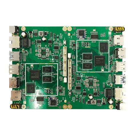
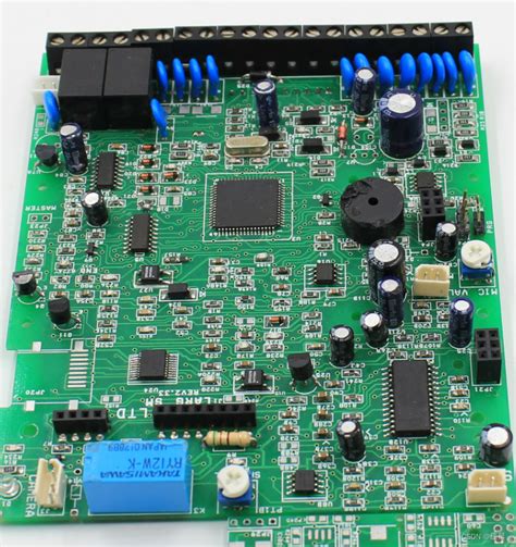
Created using similar processes to production PCBs but in small quantities, these represent the first true proto PCBs in the development sequence.
5. Milled Prototypes
Produced using CNC milling machines that mechanically remove copper to create circuit patterns, ideal for quick turnaround testing.
6. 3D Printed Electronics
An emerging technology that builds conductive traces directly onto substrates using specialized materials and printers.
Each type serves different purposes in the product development lifecycle, from initial concept validation (breadboards) to near-production testing (etched or milled prototypes).
The Proto PCB Design and Fabrication Process
Creating effective proto PCBs requires careful planning and execution through several stages:
1. Schematic Design
Engineers begin by creating a schematic diagram of the circuit using Electronic Design Automation (EDA) software. This virtual representation includes all components and their interconnections.
2. PCB Layout
The schematic is translated into a physical layout, determining component placement and routing of copper traces. Proto PCB layouts often include additional test points and may sacrifice some miniaturization for easier debugging.
3. Design Rule Check (DRC)
The layout undergoes automated verification to ensure it meets manufacturing capabilities and electrical requirements.
4. File Generation
The design software generates manufacturing files (Gerber files, drill files, etc.) that contain all necessary information for fabrication.
5. Fabrication Method Selection
Depending on requirements (speed, cost, fidelity), an appropriate prototyping method is chosen—etching, milling, or professional small-batch fabrication.
6. Assembly
Components are soldered onto the fabricated board, either manually for early prototypes or using pick-and-place machines for more advanced prototypes.
7. Testing and Iteration
The assembled proto PCB undergoes rigorous testing, with findings used to refine the design through subsequent iterations.
Advantages of Using Proto PCBs in Product Development
The use of proto PCBs offers numerous benefits throughout the electronics development process:
- Cost Efficiency: Identifying and resolving issues at the prototype stage prevents expensive rework during mass production.
- Time Savings: Parallel development of hardware and software becomes possible with functional prototypes.
- Performance Validation: Engineers can verify that the circuit behaves as intended under real-world conditions.
- Form Factor Testing: Proto PCBs allow evaluation of physical dimensions and component placement.
- Regulatory Compliance: Early testing helps identify potential issues with EMI, safety, or other regulatory requirements.
- Stakeholder Communication: Physical prototypes facilitate better communication with investors, clients, and team members.
- Manufacturability Assessment: Potential production issues can be identified and addressed before tooling for mass production.
Challenges in Proto PCB Development
Despite their advantages, proto PCBs present several challenges that engineers must navigate:
- Cost vs. Fidelity Tradeoff: Higher-fidelity prototypes that closely match production boards are more expensive to produce in small quantities.
- Lead Times: Even rapid prototyping services require some turnaround time, potentially slowing development.
- Limited Testing Scope: Some reliability tests (like long-term aging) are impractical with prototypes.
- Component Availability: Some components may be difficult to source in small quantities for prototyping.
- Skill Requirements: Creating effective prototypes requires expertise in both design and hands-on debugging.
- Design Lock-In: Early prototyping might lead to premature commitment to certain design choices.
Emerging Trends in Proto PCB Technology
The field of proto PCB development continues to evolve with several notable trends:
- Faster Turnaround Times: Improved manufacturing techniques and local service providers enable same-day or next-day proto PCB fabrication.
- Higher Density Capabilities: Advanced prototyping methods now support finer pitch components and high-density interconnects.
- Embedded Components: Prototyping techniques for boards with embedded passive and active components are becoming more accessible.
- Flexible and Stretchable Electronics: New materials enable prototyping of non-traditional circuit boards for wearable and IoT applications.
- AI-Assisted Design: Machine learning algorithms help optimize proto PCB layouts and predict potential issues.
- Sustainable Materials: Biodegradable substrates and lead-free solders are increasingly used in prototyping.
- Cloud-Based Collaboration: Teams can collaboratively design and review proto PCBs through web-based platforms.
Best Practices for Effective Proto PCB Development
To maximize the benefits of proto PCBs while minimizing potential pitfalls, engineers should follow these best practices:
- Define Clear Objectives: Determine exactly what needs to be validated with each prototype iteration.
- Start Simple: Begin with the minimum viable prototype that tests the riskiest assumptions.
- Document Thoroughly: Maintain detailed records of design choices, test procedures, and results.
- Plan for Debugging: Include test points, LED indicators, and other debugging aids in the design.
- Simulate First: Use circuit simulation software to catch obvious issues before physical prototyping.
- Standardize Components: Use readily available parts to simplify sourcing and future production.
- Iterate Strategically: Plan multiple prototype iterations with increasing complexity and fidelity.
- Consider Manufacturing Early: Ensure prototype designs consider eventual production constraints.
The Future of Proto PCB Technology
Looking ahead, several developments promise to further transform proto PCB technology:
- Additive Electronics Manufacturing: Complete 3D printing of functional circuit boards with embedded components.
- Molecular-Scale Prototyping: Techniques allowing for atomic-level modification of conductive materials.
- Self-Healing Circuits: Prototypes incorporating materials that can repair certain types of damage automatically.
- Quantum Circuit Prototyping: Methods for testing quantum computing components at practical scales.
- Neural Interface Prototyping: Specialized proto PCBs for brain-computer interface development.
- Environmental Interaction Testing: Prototypes designed specifically to evaluate performance under extreme conditions.
As these technologies mature, they will further reduce the barriers between concept and functional prototype, accelerating innovation across all fields of electronics.
Conclusion
Proto PCBs represent an indispensable tool in modern electronics development, offering a practical pathway from concept to product. Their evolution has mirrored—and in some cases driven—advancements in electronics manufacturing as a whole. By allowing for thorough testing and validation before committing to mass production, proto PCBs save companies significant time and resources while improving product quality and reliability.
As prototyping technologies continue to advance, becoming faster, more affordable, and more sophisticated, their role in electronics development will only grow more central. Engineers and designers who master the art and science of proto PCB development position themselves—and their organizations—for success in an increasingly competitive and innovation-driven marketplace.
The future of electronics will be built, one prototype at a time, on the foundation of ever-more-capable proto PCB technologies. Understanding and leveraging these tools effectively will remain a critical skill for anyone involved in bringing new electronic products to life.