Design and Implementation of Amplifier Circuit PCBs: A Comprehensive Guide
Introduction to Amplifier Circuit PCBs
Printed Circuit Boards (PCBs) form the backbone of modern electronic amplifier systems, providing the physical platform for component mounting and electrical interconnections. Amplifier circuit PCBs present unique design challenges that differentiate them from other types of electronic circuits due to their handling of analog signals, power requirements, and sensitivity to noise and interference.
The design of amplifier PCBs requires careful consideration of several factors including signal integrity, power distribution, thermal management, and electromagnetic compatibility. Whether designing for audio applications, RF systems, or instrumentation amplifiers, the PCB layout significantly impacts the performance, stability, and reliability of the final product.
This article explores the fundamental principles, design considerations, and best practices for creating high-performance amplifier circuit PCBs. We will examine various types of amplifier circuits, material selection, layout techniques, and testing methodologies to help engineers and hobbyists achieve optimal results in their amplifier PCB designs.
Types of Amplifier Circuits and Their PCB Implications
1. Audio Amplifiers
Audio amplifier PCBs typically handle signals in the 20Hz to 20kHz range and require special attention to:
- Grounding schemes to minimize hum and noise
- Proper decoupling for clean power delivery
- Signal path routing to prevent crosstalk
- Component selection for optimal sound quality
Class AB audio amplifiers, for example, need careful thermal design due to their moderate efficiency, while Class D switching amplifiers require stringent EMI control measures.
2. RF Amplifiers
Radio Frequency amplifiers operate at much higher frequencies (from several MHz up to GHz ranges) and demand:
- Controlled impedance transmission lines
- Minimal parasitic capacitance and inductance
- Careful shielding and grounding
- High-frequency laminate materials
The PCB layout for RF amplifiers often requires microstrip or stripline transmission line structures and meticulous attention to component placement.
3. Operational Amplifier Circuits
Op-amp based circuits are ubiquitous in analog electronics and require:
- Proper bypassing near power pins
- Short feedback paths
- Balanced layout for differential inputs
- Guard rings for high-impedance circuits
The relatively low power but high precision nature of op-amp circuits makes proper PCB layout crucial for maintaining signal integrity.
PCB Material Selection for Amplifier Circuits
The choice of PCB substrate material significantly affects amplifier performance:
1. Standard FR-4
- Cost-effective for audio and low-frequency applications
- Moderate dielectric constant (≈4.3-4.8)
- Suitable for most general-purpose amplifiers below 100MHz
2. High-Frequency Laminates
- Materials like Rogers RO4000 series or Teflon-based substrates
- Stable dielectric constant over frequency
- Low loss tangent for RF applications
- More expensive but necessary for high-frequency performance
3. Metal-Core PCBs
- Used for high-power amplifier circuits
- Excellent thermal conductivity
- Typically aluminum or copper core
- Specialized manufacturing requirements
4. Thick Copper PCBs
- For high-current amplifier stages
- Copper weights up to 20oz or more
- Improved current handling and thermal performance
The material selection should consider the amplifier’s frequency range, power requirements, and thermal characteristics to ensure optimal performance and reliability.
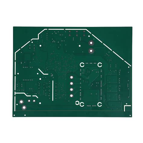
Critical PCB Layout Considerations for Amplifiers
1. Power Distribution Network Design
- Use star grounding for analog circuits
- Implement proper decoupling with multiple capacitor values
- Keep power traces short and wide
- Consider separate power planes for analog and digital sections
2. Signal Routing Techniques
- Keep input signals away from output traces
- Minimize parallel runs of input and output traces
- Use ground planes beneath sensitive traces
- Maintain consistent impedance for high-frequency signals
3. Thermal Management
- Provide adequate copper area for heat dissipation
- Use thermal vias for heat transfer to other layers
- Position heat-generating components strategically
- Consider heatsink mounting requirements
4. EMI/EMC Considerations
- Implement proper shielding where needed
- Use guard traces around sensitive nodes
- Minimize loop areas in high-current paths
- Filter I/O connections appropriately
Stage-by-Stage Amplifier PCB Layout Guidelines
1. Input Stage Layout
- Keep input traces as short as possible
- Shield sensitive input nodes
- Use guard rings for high-impedance inputs
- Maintain symmetry in differential pairs
2. Gain Stage Layout
- Provide local decoupling near active devices
- Minimize parasitic capacitance around high-impedance nodes
- Ensure proper biasing network layout
- Maintain signal path integrity
3. Output Stage Layout
- Use thick copper traces for high-current paths
- Implement star grounding near output devices
- Provide adequate heat dissipation
- Consider output protection circuitry
4. Feedback Network Layout
- Place feedback components close to the amplifier
- Minimize trace lengths in feedback paths
- Avoid routing feedback traces near noisy signals
- Maintain precision in feedback component placement
Advanced Techniques for High-Performance Amplifier PCBs
1. Mixed-Signal Layout Strategies
- Proper partitioning of analog and digital sections
- Careful ground plane design
- Strategic use of moats and bridges
- Filtered power supply distribution
2. RF-Specific Techniques
- Microstrip and stripline transmission lines
- Impedance matching networks
- Quarter-wave transformers
- Proper via stitching for shielding
3. High-Power Design Methods
- Thermal relief patterns
- Current density calculations
- Fusing and protection circuitry
- Creepage and clearance considerations
4. Low-Noise Techniques
- Star grounding implementation
- Shielding sensitive components
- Careful component selection
- Vibration-resistant mounting
Testing and Verification of Amplifier PCBs
1. Pre-Layout Simulation
- Circuit simulation with parasitic estimates
- Thermal analysis
- Signal integrity verification
- Power distribution network analysis
2. Prototype Evaluation
- Frequency response measurements
- Distortion analysis
- Noise floor assessment
- Thermal imaging under load
3. Production Testing
- Automated optical inspection (AOI)
- In-circuit testing (ICT)
- Functional testing
- Burn-in procedures for reliability
Common Pitfalls and How to Avoid Them
1. Grounding Problems
- Issue: Ground loops causing hum and noise
- Solution: Implement proper star grounding or ground plane strategies
2. Thermal Issues
- Issue: Overheating leading to premature failure
- Solution: Adequate copper pour, thermal vias, and heatsinking
3. Signal Integrity Problems
- Issue: Oscillations or frequency response aberrations
- Solution: Proper layout of feedback networks and bypassing
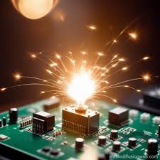
4. EMI Problems
- Issue: Radiated emissions or susceptibility
- Solution: Proper shielding, filtering, and layout techniques
Future Trends in Amplifier PCB Design
1. Integration with Digital Systems
- Embedded DSP control
- Digital pre-distortion techniques
- Smart amplifier systems
2. Advanced Materials
- Higher thermal conductivity substrates
- Embedded passives
- Flexible hybrid electronics
3. Miniaturization
- High-density interconnect (HDI) techniques
- Embedded components
- 3D packaging approaches
4. Sustainable Design
- Lead-free and halogen-free materials
- Recyclable PCB constructions
- Energy-efficient amplifier topologies
Conclusion
The design and implementation of amplifier circuit PCBs requires a thoughtful approach that balances electrical performance, thermal management, and manufacturability. By understanding the specific requirements of different amplifier types, selecting appropriate materials, and implementing sound layout practices, designers can create amplifier PCBs that deliver optimal performance and reliability.
As amplifier technologies continue to evolve alongside advancements in PCB manufacturing and materials science, designers must stay informed about new techniques and best practices. The fundamental principles of careful signal routing, proper grounding, and thermal consideration will remain essential, even as new challenges emerge in areas like high-frequency digital amplification and energy-efficient designs.
By applying the guidelines and techniques discussed in this article, engineers can overcome the common challenges in amplifier PCB design and create robust, high-performance circuits that meet the demanding requirements of modern electronic systems.