Advanced Box Build PCB Techniques for System Integration
Key Takeaways
When optimizing PCB manufacturing for system integration, you need to balance precision and scalability. Advanced box build PCB techniques focus on minimizing errors in assembly while ensuring compatibility with industrial automation workflows. For PCB manufacturing companies, this means adopting modular design principles that simplify component placement and reduce PCB manufacturing cost through standardized processes.
"Collaborating with experienced PCB manufacturing business partners ensures access to specialized tools for high-density interconnects and thermal management—key factors in industrial electronics reliability."
Implementing streamlined testing protocols—such as automated optical inspection (https://www.andwinpcba.com).
By integrating advanced automation, such as robotic soldering and AI-driven quality control, you can enhance throughput while maintaining consistency. Prioritize partnerships with PCB manufacturing providers that offer end-to-end traceability, ensuring compliance with industry standards. This approach not only future-proofs your operations but also positions your projects to leverage emerging trends like IoT-enabled assembly systems and sustainable material sourcing.
Optimizing PCB System Integration Techniques
To achieve seamless system integration in PCB manufacturing, you need to prioritize design alignment with mechanical and electrical requirements. Start by evaluating component placement to minimize signal interference while ensuring compatibility with enclosure dimensions. Thermal management becomes critical here—improper heat dissipation can compromise performance, especially in high-density layouts. Collaborating with experienced PCB manufacturing companies ensures access to precision tooling and advanced assembly techniques, such as 3D modeling for virtual fit checks before physical prototyping.
Balancing PCB manufacturing cost with functionality requires strategic material selection and process optimization. For example, using rigid-flex PCBs reduces connector counts, lowering assembly complexity and potential failure points. Consider the following comparison for traditional vs. integrated approaches:
| Factor | Traditional Assembly | Integrated Box Build |
|---|---|---|
| Component Density | Moderate | High |
| Assembly Time | Longer | Streamlined |
| Error Rate | 8-12% | <5% |
| Scalability | Limited | High |
For a PCB manufacturing business, scalability hinges on modular designs that allow easy upgrades. Implementing standardized interfaces (e.g., USB-C or modular power connectors) simplifies future expansions. Additionally, automated optical inspection (AOI) and in-circuit testing (ICT) protocols ensure consistency across batches, reducing rework costs. By integrating these strategies, you align with industrial demands for reliability while maintaining competitive PCB manufacturing cost structures.
Precision Box Build Assembly Methods
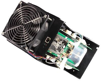
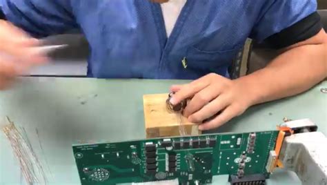
When integrating complex electronics into enclosure systems, precision begins with understanding how PCB manufacturing processes influence physical assembly. Modern high-density interconnect (HDI) PCBs demand exact alignment with mechanical components, requiring specialized jigs and fixtures to maintain positional accuracy during enclosure mounting. Leading PCB manufacturing companies now employ robotic pick-and-place systems paired with vision-guided alignment to minimize human error, particularly when handling multi-board configurations.
To optimize PCB manufacturing cost, consider modular assembly workflows that allow parallel processing of subsystems. For instance, pre-testing power distribution boards before final integration reduces rework cycles. Advanced thermal management techniques, such as laser-cut heat sinks or conformal shielding, ensure components operate within tolerance ranges even in tightly packed enclosures. This approach not only enhances reliability but also streamlines scalability for high-volume PCB manufacturing business models.
Critical to precision is traceability. Implementing RFID tagging or QR-code tracking at each assembly stage lets you monitor component origins and assembly parameters, vital for compliance in regulated industries. By aligning these methods with your PCB manufacturing strategy, you create a foundation for error-resistant system integration—a necessity for industrial applications where downtime translates directly to operational losses.
Streamlined Testing for Industrial Electronics
When optimizing industrial electronics production, implementing streamlined testing protocols becomes critical for maintaining both quality and speed. Modern automated optical inspection (AOI) and in-circuit testing (ICT) systems enable rapid fault detection without compromising PCB manufacturing cost objectives. Leading PCB manufacturing companies now deploy modular test platforms that adapt to varying product configurations, allowing you to scale operations while preserving accuracy. By integrating these systems directly into assembly lines, you reduce downtime between PCB manufacturing stages, creating a seamless workflow from component placement to final validation. Real-time diagnostics tools provide immediate feedback loops, catching defects 30% faster than manual methods. This approach not only safeguards reliability but also aligns with lean manufacturing principles by minimizing material waste. For PCB manufacturing business models targeting high-mix production, adopting AI-driven predictive analytics further refines test parameters based on historical performance data. Such integration ensures your testing framework evolves alongside advancing component technologies, future-proofing your quality assurance processes without exponential cost increases.
Scalable Solutions for Electronics Manufacturing
When scaling PCB manufacturing operations, you need strategies that balance flexibility with cost-efficiency. Leading PCB manufacturing companies achieve this by integrating modular design principles, enabling rapid adaptation to fluctuating production demands. By standardizing component layouts and assembly workflows, you reduce PCB manufacturing cost while maintaining precision—critical for high-volume industrial applications.
A key approach involves automated panelization, which optimizes material usage and accelerates throughput. This method aligns with lean manufacturing practices, minimizing waste without compromising quality. For businesses aiming to expand their PCB manufacturing business, investing in scalable testing protocols—such as inline automated optical inspection (AOI)—ensures consistent output even as order volumes spike.
Equally important is adopting reconfigurable assembly lines. These systems allow seamless transitions between product variants, catering to diverse client requirements. Partnering with suppliers that offer scalable raw material sourcing further mitigates supply chain risks. By focusing on these strategies, you create a foundation where growth doesn’t sacrifice reliability—a non-negotiable in industrial electronics.
Transitioning to scalable solutions isn’t just about technology; it’s about building partnerships with PCB manufacturing companies that prioritize adaptive workflows, ensuring your operations stay agile in evolving markets.
Enhancing Manufacturing Efficiency Through Integration
Integrating PCB manufacturing processes with box build assembly creates a seamless workflow that eliminates bottlenecks in industrial electronics production. When design-for-manufacturability (DFM) principles align with system integration goals, you reduce PCB manufacturing cost by minimizing rework and material waste. For example, collaborating early with PCB manufacturing companies ensures component placement optimizes both board functionality and final enclosure fitment. This coordination becomes critical when scaling operations, as automated testing protocols validate signal integrity and mechanical stability before full system assembly.
Leveraging digital twin simulations further tightens this integration. By modeling how PCB manufacturing business decisions—like substrate selection or connector types—affect thermal management and EMI shielding, you preemptively address compatibility issues. Transitioning to unified software platforms bridges gaps between PCB fabrication data and box build BOMs, enabling real-time adjustments that maintain throughput. Modular designs, paired with standardized interfaces, allow PCB manufacturing teams to replicate proven configurations across product lines without reinventing workflows. This approach not only accelerates time-to-market but also ensures scalability as demand grows.
Ultimately, the synergy between PCB manufacturing expertise and system integration strategies transforms fragmented processes into cohesive, high-yield operations. By prioritizing cross-functional collaboration and data-driven decision-making, you unlock efficiencies that resonate across the entire production lifecycle.
Advanced Automation in Box Build Processes
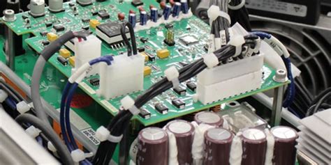
When integrating advanced automation into box build PCB systems, you’re not just streamlining workflows—you’re redefining precision. Modern PCB manufacturing leverages robotic assembly lines to handle intricate tasks like component placement, soldering, and connector integration with micron-level accuracy. This reduces human error and accelerates production cycles, directly lowering PCB manufacturing cost while maintaining consistency. For PCB manufacturing companies, adopting automated optical inspection (AOI) systems ensures defects are caught early, minimizing rework and material waste.
Automation also enhances scalability. Modular robotic systems allow rapid reconfiguration for diverse product lines, making it easier to adapt to shifting demands in the PCB manufacturing business. By pairing automation with IoT-enabled monitoring, you gain real-time adjustments to assembly parameters, ensuring optimal performance across temperature, vibration, and electrical testing phases. This synergy between hardware and software creates a closed-loop system where data drives continuous improvement.
Transitioning to automated processes isn’t just about speed—it’s about building reliability into every stage. From automated guided vehicles (AGVs) transporting assemblies to AI-driven predictive maintenance, these technologies future-proof your operations while aligning with industrial efficiency goals. The result? A seamless bridge between PCB manufacturing precision and scalable, error-resistant system integration.
Ensuring Reliability in Box Build Systems
When integrating PCB manufacturing into box build assemblies, reliability hinges on three pillars: component selection, process validation, and environmental resilience. You’ll need to verify that PCB manufacturing companies adhere to stringent quality standards, particularly for high-density interconnects or mixed-signal designs. Thermal management becomes critical here—improper heat dissipation in tightly packed systems can accelerate component degradation, raising long-term PCB manufacturing cost due to premature failures.
To mitigate risks, implement automated optical inspection (AOI) during assembly to catch soldering defects early. Partnering with PCB manufacturing business experts ensures traceability, from raw material sourcing to final testing protocols like accelerated life testing. This approach not only validates durability under extreme conditions but also aligns with scalable production workflows.
Don’t overlook mechanical stability—vibration-resistant mounting and conformal coatings protect against physical stressors common in industrial environments. By balancing PCB manufacturing cost with robust design practices, you create systems that endure operational demands while maintaining efficiency. Remember, reliability isn’t a single checkpoint; it’s woven into every layer of integration.
Future Trends in PCB Box Build Technology
As industrial demands evolve, PCB manufacturing will increasingly rely on smart automation and data-driven design. Expect PCB manufacturing companies to adopt AI-powered inspection systems that predict assembly errors in real time, reducing PCB manufacturing costs by minimizing rework. Modular architectures will dominate, allowing you to scale PCB manufacturing business operations without overhauling existing infrastructure.
Another key shift involves sustainable practices—think biodegradable substrates and energy-efficient assembly lines. These innovations not only align with global regulations but also cut long-term operational expenses. Meanwhile, hybrid models combining rigid-flex PCBs with embedded sensors will enhance system diagnostics, ensuring reliability in harsh environments.
You’ll also see tighter integration between PCB manufacturing and IoT ecosystems. Edge computing modules, for instance, will be pre-integrated during box builds to streamline deployment. To stay competitive, prioritize partnerships with PCB manufacturing companies specializing in high-mix, low-volume production—this flexibility is critical as customization becomes the norm.
Finally, advancements in 3D printing for enclosures and connectors will shorten prototyping cycles, enabling faster time-to-market. By aligning with these trends, you’ll future-proof your systems while maintaining cost-efficiency and scalability.
Conclusion
As you evaluate advanced box build PCB techniques, understanding their role in optimizing PCB manufacturing workflows becomes essential. Modern system integration demands a balance between PCB manufacturing cost and precision—whether through automated assembly processes or rigorous testing protocols. Leading PCB manufacturing companies now leverage scalable solutions to ensure production flexibility, enabling your PCB manufacturing business to adapt to fluctuating demands without sacrificing quality.
By adopting modular designs and predictive maintenance frameworks, you can reduce downtime while maintaining reliability across industrial applications. These strategies not only streamline assembly but also future-proof operations against evolving technological standards. As you look ahead, prioritizing partnerships with suppliers who align with your integration goals ensures seamless transitions from prototyping to full-scale production. Remember, the true value of advanced box build systems lies in their ability to unify design, assembly, and testing into a cohesive, cost-effective workflow—a critical advantage in today’s competitive electronics landscape.
Frequently Asked Questions
How does box build PCB integration improve system reliability?
By combining PCB manufacturing with mechanical assembly, box build techniques ensure components interact seamlessly. Precision alignment reduces signal interference, while integrated testing protocols catch defects early—critical for industrial applications demanding zero-failure performance.
What factors influence PCB manufacturing cost in box build projects?
Material selection, assembly complexity, and testing rigor directly affect costs. Working with experienced PCB manufacturing companies helps optimize designs for scalability and cost-efficiency, balancing high-quality components with budget constraints.
How do you choose the right PCB manufacturing business for box build systems?
Look for providers with expertise in end-to-end integration, including DFM (Design for Manufacturing) analysis and automated testing. Certifications like ISO 9001 and IPC-A-610 compliance indicate adherence to industrial-grade reliability standards.
Can PCB manufacturing timelines align with rapid prototyping needs?
Yes. Many companies offer accelerated prototyping services, leveraging modular designs and pre-validated subsystems. This approach minimizes delays while maintaining manufacturing efficiency—key for industries like automotive or IoT.
What role does automation play in modern box build processes?
Automated optical inspection (AOI) and robotic soldering ensure micron-level precision, reducing human error. This is particularly vital for high-volume PCB manufacturing, where consistency directly impacts system uptime and lifecycle costs.
Ready to Optimize Your Box Build Project?
For tailored solutions that align with your PCB manufacturing cost and quality goals, click here to explore Andwin PCB’s expertise. Their end-to-end services streamline integration from design to delivery.