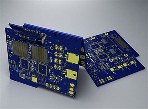
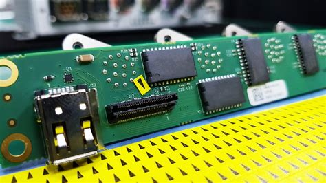
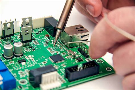
How to Reduce PCB Electromagnetic Interference (EMI)
Introduction
Electromagnetic interference (EMI) is a critical concern in modern printed circuit board (PCB) design, affecting the performance, reliability, and regulatory compliance of electronic devices. As electronic systems become more complex and operate at higher frequencies, managing EMI has become increasingly challenging. This article explores comprehensive strategies to reduce PCB electromagnetic interference, covering design principles, layout techniques, component selection, and shielding methods.
Understanding EMI in PCBs
EMI refers to the disruption of electronic device operation caused by electromagnetic radiation or conduction from another device. In PCBs, EMI manifests in two forms:
- Radiated EMI: Electromagnetic waves propagating through air
- Conducted EMI: Unwanted signals traveling through power and ground connections
Common sources of EMI in PCBs include:
- High-speed digital circuits
- Switching power supplies
- Clock signals
- RF circuits
- High-current traces
Fundamental Design Principles for EMI Reduction
1. Proper Grounding Techniques
Grounding is the foundation of EMI control in PCB design:
Single-Point Grounding: Effective for low-frequency circuits (<1MHz), where all ground connections meet at one physical location to prevent ground loops.
Multi-Point Grounding: Preferred for high-frequency circuits (>10MHz), creating multiple connections to a low-impedance ground plane to minimize ground impedance.
Ground Plane Implementation:
- Use solid ground planes whenever possible
- Maintain ground plane continuity (avoid splits under critical traces)
- For multilayer boards, dedicate entire layers to ground
2. Power Distribution Network Design
A well-designed power distribution network (PDN) significantly reduces EMI:
- Implement power planes similar to ground planes
- Use appropriate decoupling capacitors:
- Place bulk capacitors near power entry points
- Use smaller value capacitors close to IC power pins
- Follow manufacturer recommendations for capacitor values
- Consider using ferrite beads for high-frequency noise filtering
3. Signal Routing Strategies
Proper signal routing minimizes electromagnetic emissions:
Trace Geometry:
- Keep traces as short as possible
- Use appropriate trace widths for current requirements
- Avoid sharp right-angle bends (use 45° angles or curves)
Differential Signaling:
- Implement differential pairs for high-speed signals
- Maintain consistent spacing and length matching
- Route differential pairs close to each other
Impedance Control:
- Match trace impedance to source and load
- Use controlled impedance routing for high-speed signals
- Consider microstrip or stripline configurations
Advanced PCB Layout Techniques
1. Component Placement Optimization
Strategic component placement reduces EMI:
- Group components by function (digital, analog, power, etc.)
- Place high-speed components away from board edges
- Position clock generators centrally to minimize trace lengths
- Orient components to minimize trace crossings
2. Layer Stackup Design
Proper layer stackup is crucial for EMI control:
4-Layer Board Example:
- Top layer: Signals and components
- Inner layer 1: Ground plane
- Inner layer 2: Power plane
- Bottom layer: Signals and components
6-Layer Board Example:
- Top layer: Signals and components
- Ground plane
- Signal layer (high-speed)
- Power plane
- Ground plane
- Bottom layer: Signals and components
Key considerations:
- Place ground planes adjacent to signal layers
- Maintain symmetry in the stackup
- Use thin dielectrics between power and ground planes for better decoupling
3. Clock and High-Speed Signal Management
Clock signals are major EMI sources:
- Use lowest acceptable clock frequency
- Implement spread spectrum clocking when possible
- Route clock signals first, keeping traces short and direct
- Avoid vias in clock traces when possible
- Use guard traces or ground shielding for critical clocks
4. Partitioning and Isolation
Physical separation of circuit types reduces interference:
- Separate analog and digital sections
- Isolate high-power and sensitive circuits
- Create moats (physical gaps) between sections when necessary
- Use separate ground planes for different circuit types with controlled connections

Component Selection for EMI Reduction
1. IC Selection Considerations
- Choose devices with built-in EMI reduction features
- Prefer devices with slower edge rates when possible
- Select packages with good power and ground connections
- Consider ICs with spread spectrum capabilities
2. Passive Components
- Use surface-mount devices (SMDs) for better high-frequency performance
- Select capacitors with low equivalent series resistance (ESR)
- Choose ferrite beads appropriate for the frequency range of concern
- Use common-mode chokes for differential interfaces
3. Connectors and Cabling
- Use shielded connectors for sensitive interfaces
- Implement proper pin assignment (separate high-speed and low-speed signals)
- Consider filtered connectors for I/O ports
- Use twisted-pair or shielded cables when appropriate
Shielding and Filtering Techniques
1. PCB-Level Shielding
- Implement ground stitching vias around board perimeter
- Use copper fills in unused board areas (tied to ground)
- Consider localized shielding cans for critical circuits
- Implement proper shield grounding (multiple connections for high frequencies)
2. Filter Implementation
- Use pi-filters for power supply inputs
- Implement EMI filters on all I/O lines
- Consider common-mode filters for differential interfaces
- Use feedthrough capacitors for high-frequency filtering
3. System-Level Shielding
- Design enclosures with proper conductive gasketing
- Maintain continuous conductivity across seams
- Implement proper shield grounding strategy
- Use absorptive materials for resonant frequencies
Testing and Verification
1. Pre-Compliance Testing
- Conduct near-field scans during development
- Use spectrum analyzers to identify emission sources
- Perform time-domain reflectometry (TDR) for impedance verification
2. Design Rule Checking
- Implement automated EMI design rule checks (DRC)
- Verify clearance and creepage distances
- Check for proper return paths
3. Iterative Design Process
- Build prototypes early
- Test and measure EMI performance
- Implement corrective measures
- Repeat until requirements are met
Regulatory Considerations
Understanding EMI standards is essential for compliance:
- FCC Part 15 (United States)
- CISPR 22/32 (International)
- EN 55022/32 (European Union)
- Military standards (MIL-STD-461)
Design with compliance in mind from the beginning to avoid costly redesigns.
Emerging Technologies and Future Trends
1. Advanced Materials
- High-frequency laminates with controlled dielectric properties
- Embedded capacitance materials
- Nanocomposite shielding materials
2. Design Tools
- 3D electromagnetic simulation software
- AI-assisted layout optimization
- Real-time EMI analysis tools
3. Novel Techniques
- Electromagnetic bandgap structures
- Metamaterials for EMI suppression
- Active cancellation technologies
Conclusion
Reducing PCB electromagnetic interference requires a systematic approach encompassing proper design principles, careful layout techniques, appropriate component selection, and effective shielding methods. By implementing these strategies from the initial design phase, engineers can significantly improve EMI performance, reduce development time, and ensure regulatory compliance. As electronic systems continue to evolve with higher speeds and greater complexity, EMI mitigation will remain a critical aspect of successful PCB design.
Remember that EMI control is not just about solving problems but preventing them through good design practices. A well-designed PCB with proper EMI considerations will not only pass compliance testing but also exhibit better signal integrity, lower noise, and improved overall reliability. By mastering these techniques, designers can create electronic products that perform optimally in increasingly crowded electromagnetic environments.